KE-3010_SPE_EN - 第39页
- 34 - 5.2.14. Coplanarity (Factory - Set O ption) By moving a tar get component that is to be measured at constan t speed in the direction (Y - dir ection) perpendicular to the laser line (X - direction), the camera sho…
- 33 -
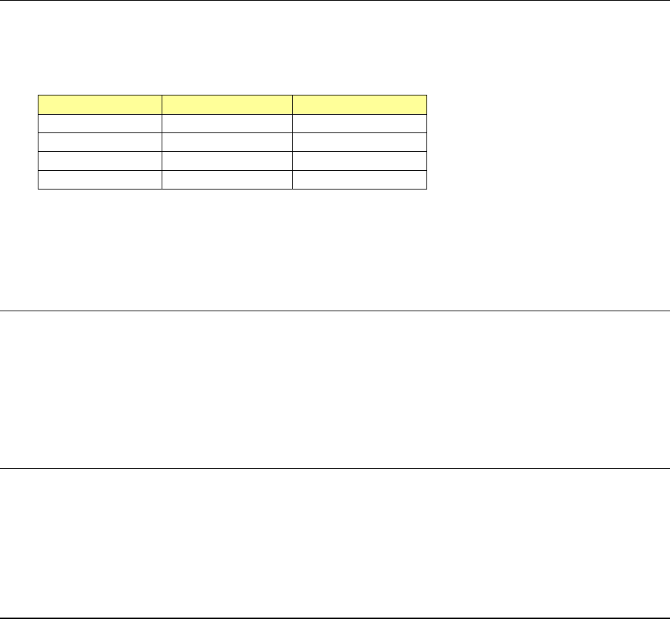
5.2.10. Applicability to long PWB (factory-set option)
The PWB size in the X direction can be extended by PWB twice-feed transport. This
permits producing long PWBs to be used for LED lighting. With the PWB exceeding the
single-feed size of the maximum size in the X direction shown in the following table,
twice-feed transport is performed.
Single-feed
Twice-feed
M PWB
330×250mm
650x250mm
L PWB
410×360mm
800×360mm
L-Wide PWB
510×360mm
1010×360mm
XL PWB
610×560mm
1210×560mm
Re
strictions
- The IN buffer/OUT buffer function is disabled.
- When MTC is used, a limitation is put on the maximum PWB size in the X direction that
can be transported.
5.2.11. Solder recognition lighting (factory-set option)
When there is no BOC mark on a PWB or circuit, the solder print is recognized as a BOC
mark. When executing twice-feed transport of long PWBs, the placement pad for which
solder print is performed can be used as a BOC mark in placement in a range without any
BOC mark.
*
I
n the case of the solder print, the shape is not clear as a mark, so that satisfactory
placement accuracy may not be obtained.
5.2.12. Residual number-of-components control function (option)
This function controls product lots of placement components (LED components, etc.). The
function checks whether the necessary number of placement components exists in the
feeder in carrying in PWBs without mixing different-lot components into the same PWB. If
the number is less than the necessary number, an alarm is displayed before placement is
started.
5.2.13. Auto PWB width adjusting function (Automatic Board Adjustment/AWC
factory-set option)
This function can adjust the rail width automatically according to the PWB width.
The minimum value of applicable PWB dimensions is 50mm x 50 mm.
- 34 -
5.2.14. Coplanarity (Factory-Set Option)
By moving a target component that is to be measured at constant speed in the direction
(Y-direction) perpendicular to the laser line (X-direction), the camera shoots the diffuse
reflection of laser beam emitted to the component and the device creates 3-D image to
measure displacement without touching the component. This device determines if a
component is appropriate or not based on the 3-D image obtained from the component
information sent by the mounter in advance (that is, checks the height of the electrode).
Accordingly, lead bend in the up/down direction of a lead component or a nick of a ball
component can be recognized, thereby preventing a contact fault between a PWB and a
component.
Colinearity check:
The colinearity check inspects “how much a side on which leads are located is bent in the
up/down directions.”
Coplanarity check:
This check can check coplanarity (uniformity of the bottom of a terminal) of a component with
the three-point method (JEDEC standard: JESD22-B108A) or the method of least squares
(JEDEC standard: JESD22-B108A).
A
pplicable components
- Components to be recognized with a VCS only.
- BGA, FBGA, connector, and lead components (SOP and QFP) whose respective pitch
is the same and whose respective lead width is the same
*
1. If you do not enter the correct lead width and electrode size of a component whose
lead width is less than 0.3 mm on the “Component” data screen of the Program Editor,
the system may not be able to detect its terminal correctly.
*2. Component height:SC specification: 6 mm, NC specification: 12 .0 mm
HC specification: 20.0mm, EC specification:25.0mm
A product whose laser class is 3b is used in the coplanarity sensor.
- K
ey switch
The front section of the machine is equipped with a key switch. Only when the key
switch is set to ON, you can use the coplanarity function.
- Cover open
Regardless of the key switch state, any laser is not emitted when the cover opens.
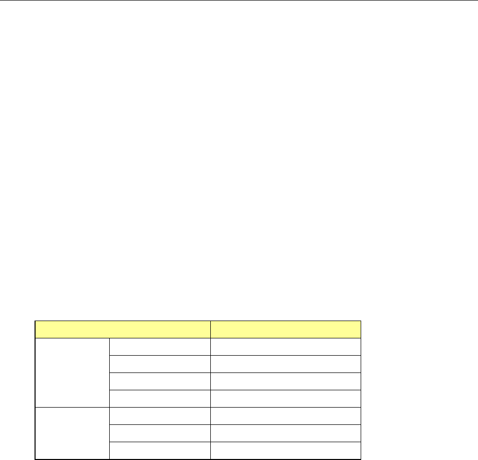
Item
Dimensions
Lead
component
Pitch 0.4 mm or more
Lead width
*1
0.18 mm or more
Lead length 0.5 mm or more
Component size 48 mm×150 mm or less
Ball
component
Pitch 0.8 mm or more
Ball diameter 0.4 mm or more
Component size 48 mm×150 mm or less
- 35 -
5.2.15. Offset Placement After Solder Screen-printing (Factory-Set Option)
A component placement position error may occur after re-flowing if you place a component
on the PWB pad when the solder printing position is shifted from the pad position because a
PWB expands or shrinks.
This function uses an OCC to recognize a gap between a PWB pad and printed solder that is
generated as a result of expansion and/or contraction of a PWB, and places a component on
the printed solder instead of the pad. This makes use of the self-alignment effect to
improve the component placement accuracy after re-flowing.
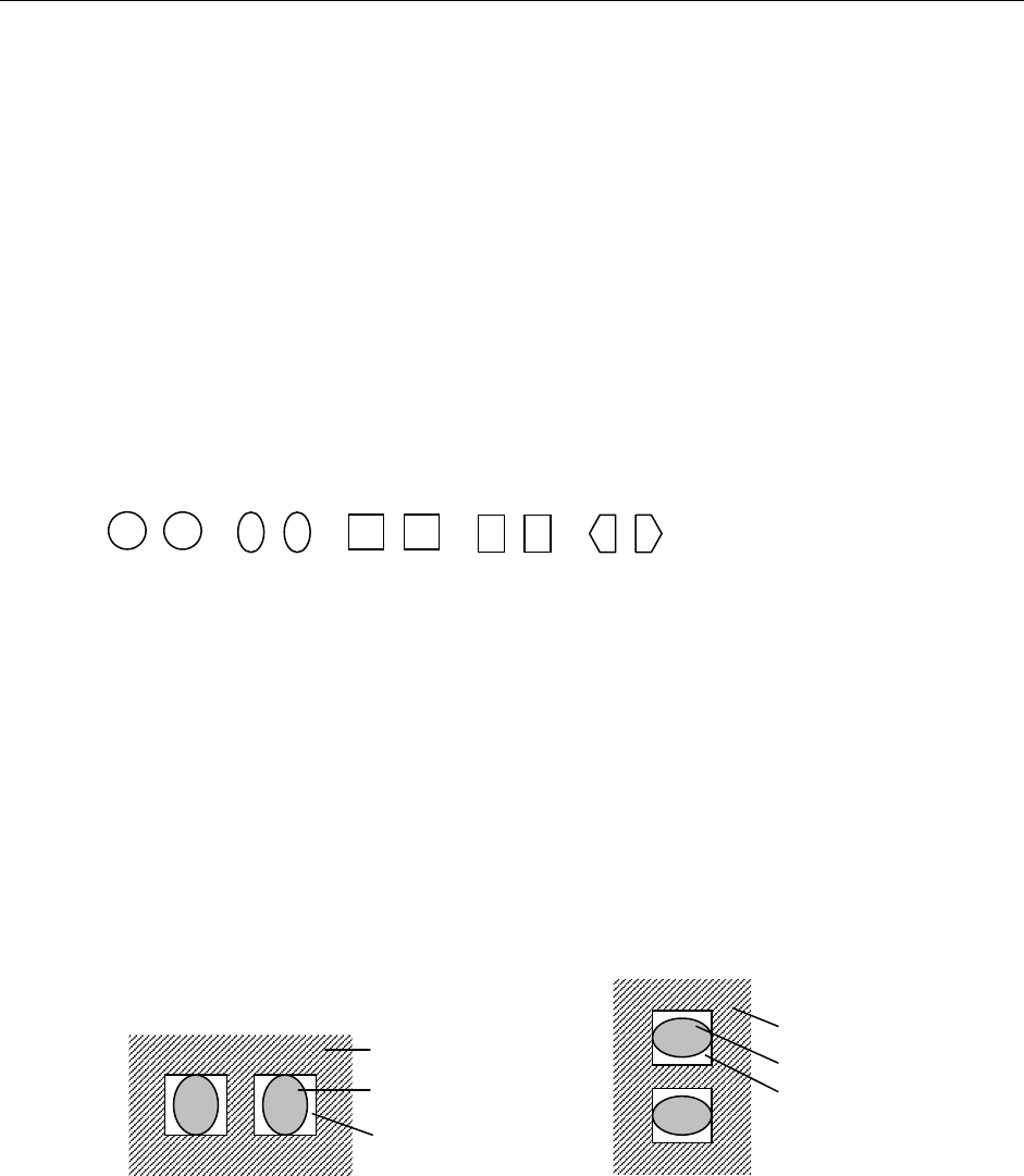
① Applicable solder shape
A pair of cream solders, which are symmetrical, screen-printed on a PWB pad for a
square chip
* The shape of screen-printed solder should be symmetrical. The system cannot
accurately detect how much to correct the gap unless the shape is symmetrical.
The applicable shapes should be: circle, oval, square, rectangle and pentagon.
(Recognition of other shapes should be checked.)
② A
pplicable solder
Eutectic solder (NIHON HANDA: RX363-92MY0 (S)) and lead-free solder (TAMURA
KAKEN: TFL-204F-111S)
(* Solder described in parentheses is already checked for its appropriateness.)
③ Applicable chip size
0402, 0603, 1005, 1608, 2012, 3216
* Note that image of a set of solder whose shorter side is 0.16 mm or more and whos
e
longer side is 3.2 mm or less has to be obtained.
④ A
pplicable solder angle
0°, 90°, 180°, 270° (Angle error for a camera: within ± 3°)
<Solder angle: 0° or 180°> <Solder angle: 90° or 270°>
⑤ A
pplicable board material and pad material
− Board material: glass epoxy, paper phenol, flexography, ceramic
− Pad material: gold, copper, hot air leveling
* The solder paste should have a certain level of contrast. If there is a portion whose
br
ightness is the same as that of solder in the area to be detected due to the condition of the
printed solder, serigraph, a pattern or PWB, and so any image that only solder looks bright
cannot be obtained, the system may not be able to correct the component placement
position by recognizing it. In such a case, you have to set the position of solder paste again
so that it can have the certain level of contrast.
PWB
Solder
Pad
PWB
Solder
Pad