GD450 说明书(中英文版) - 第36页
- 3 6 - 图 3- 10 【 PCB Mark 点到边距离】 Pix 3- 10 (the distance b etween PCB mark and side) 图 3- 10 是 PCB Mark 点到边的距离,输入后搜索 PCB Mark 点时,所选的 PCB Mark 点能直接出现在视域里; It is th e d ist ance between PCB mark and side sho w in the pix …
- 35 -
PCB and stencil mark spot.
a.(挡板气缸):开启/关闭停板气缸;
( board limit cylinder):Turn on /turn off board limit cylinder
b.(运输开关):开启/关闭运输传送带;
(transmission switch): Turn on /turn off transmission belt
c.(压板到位):开启/关闭导轨压板;
(pressing plate in place): Turn on /turn off the pressing plate of the rail
d.(平台顶板):平台顶起 PCB 上升到取像位置;
(platform lifts the board): Platform lifts the PCB to the position of capturing image.
e.(平台松板):平台从取像位置下降到进板高度(Z 轴回到原点);
(platform declines the board): Platform declines to the boarding height(Z axis return to
the origin)
f.(导轨夹紧):开启/关闭导轨夹紧 PCB;
(rail clamps): Turn on /turn off that rail clamps PCB
g.(PCB 吸板阀):开启/关闭真空吸盘/吸腔,吸住 PCB;
(PCB suction valve): Turn on /turn off the vacuum sucker/suction chamber, suck PCB
h.(网框固定阀):开启/关闭钢网固定气缸与夹紧气缸;
(frame fixed valve): Turn on /turn off stencil fixed cylinder and clamping cylinder.
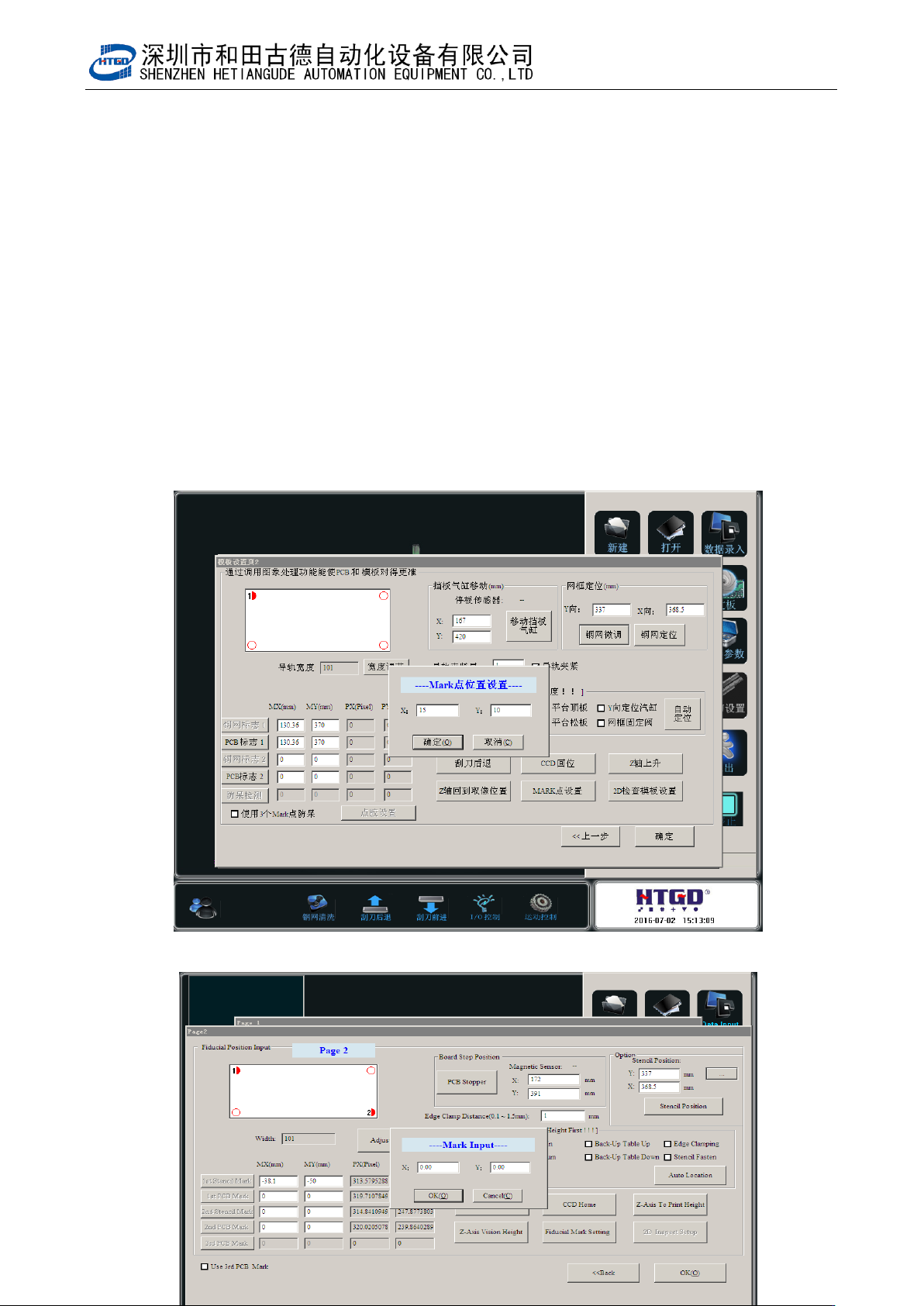
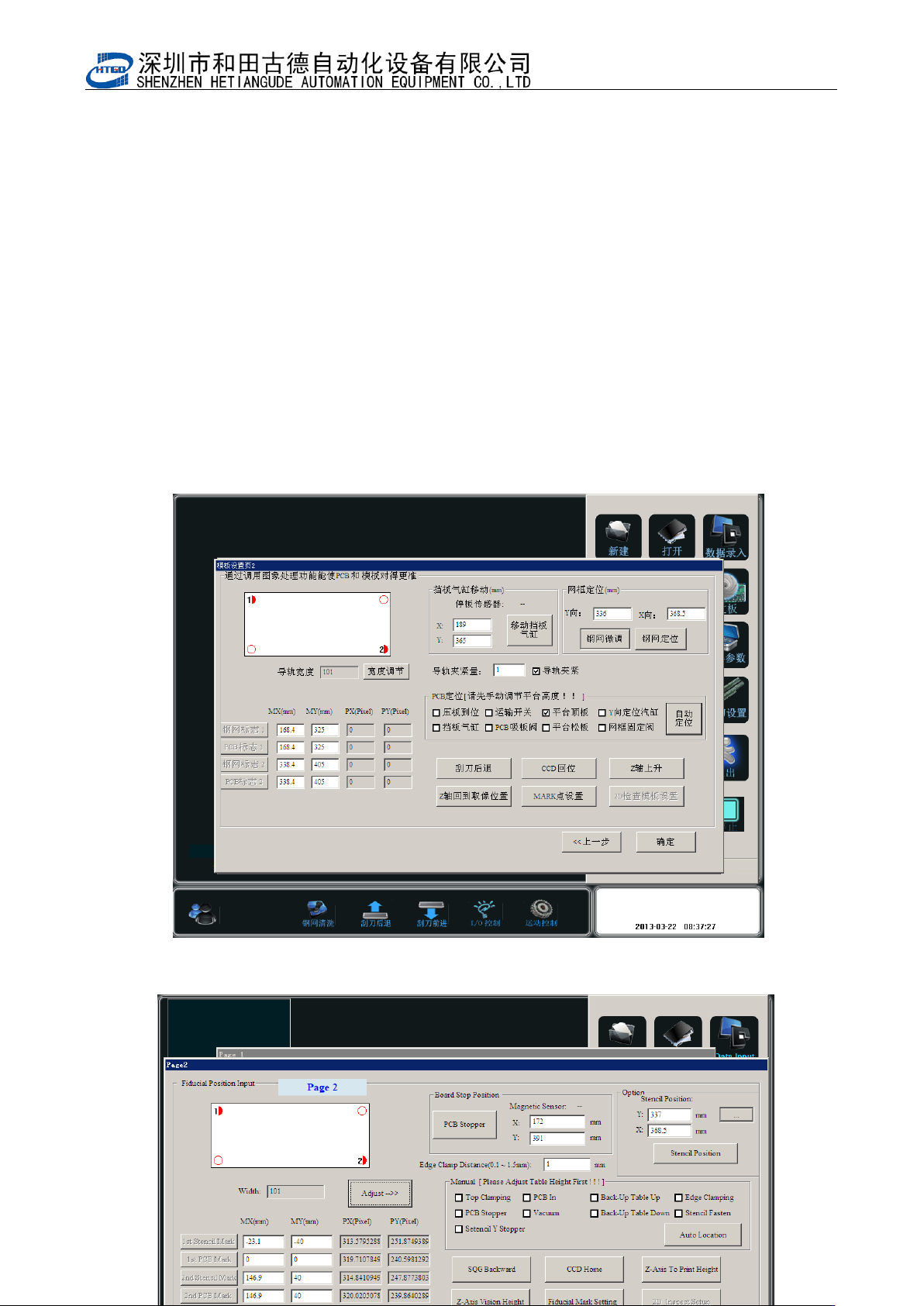
8. 3-9 画面左上角白色方框内的 4 个圆圈表示 PCB 或钢网的 4 个 Mark 点。一般我们选
择 2 个对角的点进行匹配即可。通常情况下,为了在搜索马克点时 Mark 点能出现在
CCD 的视域里,我们需要在选择匹配的 Mark 点时输入 Mark 点到边的距离,如图 3-10,
3-11 所示。
The four cycles in the white box which is in the top left corner of pix 3-9 represent
the four mark points of PCB or stencil. Usually select two diagonal points to match.
In general, in order the mark point can exist in the view of the CCD when search it,
operator needs input the distance data between mark point and side when select
the matching mark points. See pix 3-10 and 3-11.
- 36 -
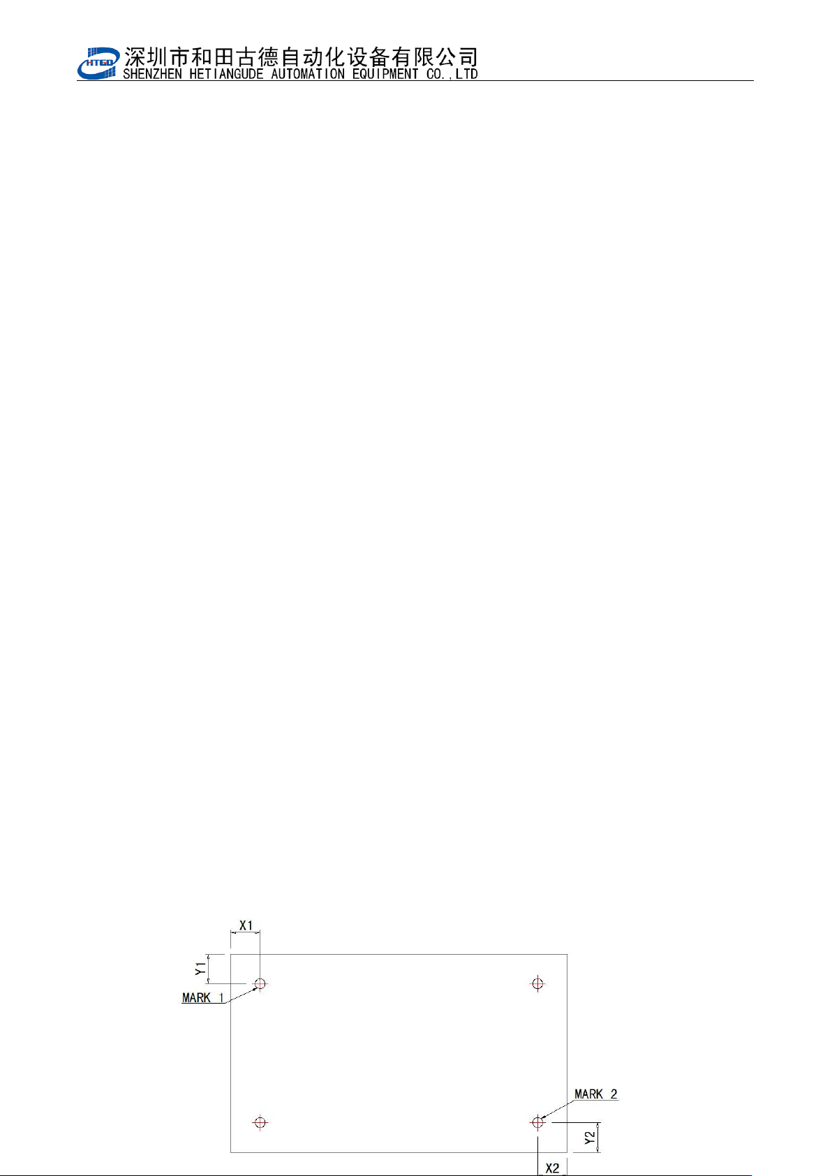
图 3-10【PCB Mark 点到边距离】
Pix 3-10(the distance between PCB mark and side)
图 3-10 是 PCB Mark 点到边的距离,输入后搜索 PCB Mark 点时,所选的 PCB Mark
点能直接出现在视域里;
It is the distance between PCB mark and side show in the pix 3-10. Input the distance
date when search the PCB mark point, the selected PCB mark point can show in the
field of vision.
图 3-11(输入 PCB Mark 点到边距离,尺寸关系参考图 3-10)
- 37 -
Pix 3-11(input the distance data between PCB mark point and side. The size relationship in
pix 3-10 is for the reference.)
图 3-12(PCB 定位)