00197498-03_UM_SiplaceCA-Serie_EN.pdf - 第204页
4 SIPLACE Wafer System (SWS) User Manual SIPLACE CA- Series 4.1 Functions From software version SC.708.0 Edition 12/2014 204 4.1.3.3 Die Recognition and Positioning The wafers are fixe d to the wafer foil with a specific…
User Manual SIPLACE CA-Series 4 SIPLACE Wafer System (SWS)
From software version SC.708.0 Edition 12/2014 4.1 Functions
203
4.1.3.2 Die Attach Process
The optional die attach unit is needed for the die attach process.
In this method, the die is placed in the same bottom/top orientation as it was on the wafer foil
("face-up" placement).
Die attach is the conventional die placement procedure. It requires an additional step in order to
establish the connection from the die to the board (wire connections).
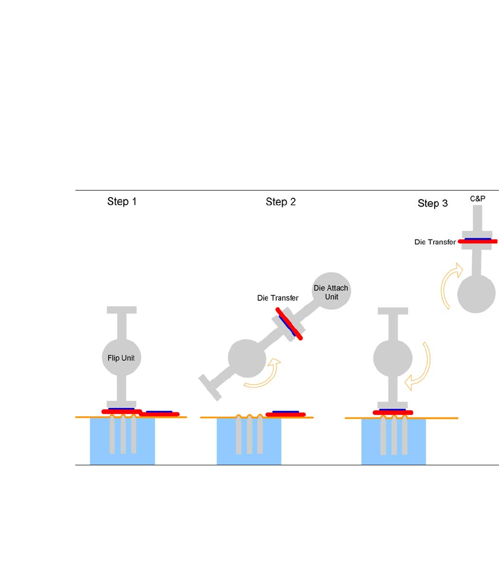
Fig. 4.1 - 3 The die attach process steps
The die attach process steps are:
– Step 1: Die release
– Step 2: The die is rotated by approx. 130°and transferred to the die attach unit.
– Step 3: The die attach unit rotates the die into the pickup position and transfers it to the place-
ment head. Parallel to this, the next die is picked up by the flip unit.
4 SIPLACE Wafer System (SWS) User Manual SIPLACE CA-Series
4.1 Functions From software version SC.708.0 Edition 12/2014
204
4.1.3.3 Die Recognition and Positioning
The wafers are fixed to the wafer foil with a specific position and angular tolerance.
It is therefore not possible to place the die reliably in the center of the ejector unit without recog-
nition and correction. This is particularly important for small dies, in order to ensure reliable ejec-
tion.
Furthermore, you may need to process only a selection of dies. A selection can be made by mark-
ing "bad" dies with an ink spot or by using a wafer map file for the relevant wafer.
The following equipment is required for this step:
2 axes wafer table for positioning
Wafer camera system for the die and for optional ink spot recognition
Optional wafer map system
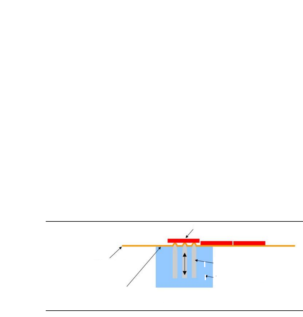
4.1.3.4 Ejection Process
Once the die has been centered using the ejection system, it can be released from the wafer foil
using needles and transferred to the flip unit. While the needles release the die from the foil, the
wafer foil is moved towards the ejection system by means of suction.
Fig. 4.1 - 4 Die presentation process
The following equipment is required for this method:
– Ejector system with exchangeable ejector tool
Ejection needle
Vacuum cap
Ejection system
Active component - ready for pickup
Wafer foil
The wafer foil is sucked up by vacuum
at the vacuum cap

User Manual SIPLACE CA-Series 4 SIPLACE Wafer System (SWS)
From software version SC.708.0 Edition 12/2014 4.1 Functions
205
4.1.3.5 Pickup Process
During the pickup process, the die is transferred to the tool or to the nozzle of the flip unit. The flip
unit transfers the die on it either to the placement head (flip chip process) or to the die attach unit
(die attach process).
The die attach unit rotates the die again and then presents it to the placement head.
The following equipment is required for this step:
Flip Unit
Die Attach Unit (optional)
4.1.4 Embedded Wafer Level Ballgrid Array (eWLB/WLFO) Process
Embedded Wafer Level Ball Grid Array is a packaging technology which allows you to produce
thin components with excellent electrical conduction, using a chip fan out solution. This means
that the area used for the connection pads is larger than the actual silicium, thereby creating con-
tact distances suitable for SMD.
For this process, the chip components are placed with the active surface face down on a carrier
with double-adhesive foil. This structure is molded after placement. After the die bonding process
on the carrier, wafer structuring processes are used to create the electrical contacts. The mold
area around the silicium is used as the carrier for the "conductive paths" (fan out). The compo-
nents are then tested, labeled and packaged i.e. in tapes.