00197498-03_UM_SiplaceCA-Serie_EN.pdf - 第207页
User Manual SIPLACE CA-Series 4 SIPLACE Wafer System (SWS) From software version SC.708.0 Edition 12/20 14 4.1 Functions 207 4.1.5 Pick & T ransfer Process in Detail 4.1.5.1 Flip Chip Segment 1 (Nozzle) 4 Fig. 4.1 - …
4 SIPLACE Wafer System (SWS) User Manual SIPLACE CA-Series
4.1 Functions From software version SC.708.0 Edition 12/2014
206
4
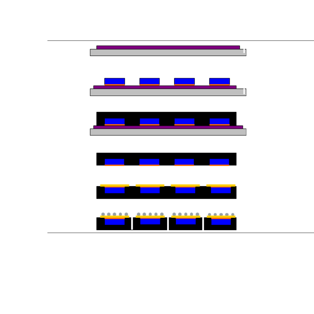
Fig. 4.1 - 5 Steps in the Embedded Wafer Level Ballgrid Array process
(1) Laminate thermal release tape on the metal carrier
(2) Make sure that the active side to be placed by the wafer (Flip Chip) faces down onto the
thermal release tape
(3) Molding under pressure; hardening at 150°C
(4) Release
(5) Re-Distribution Layer (RDL)
(6) Balling & single
(7) Testing, labeling, packing
1
2
3
4
5
6
User Manual SIPLACE CA-Series 4 SIPLACE Wafer System (SWS)
From software version SC.708.0 Edition 12/2014 4.1 Functions
207
4.1.5 Pick & Transfer Process in Detail
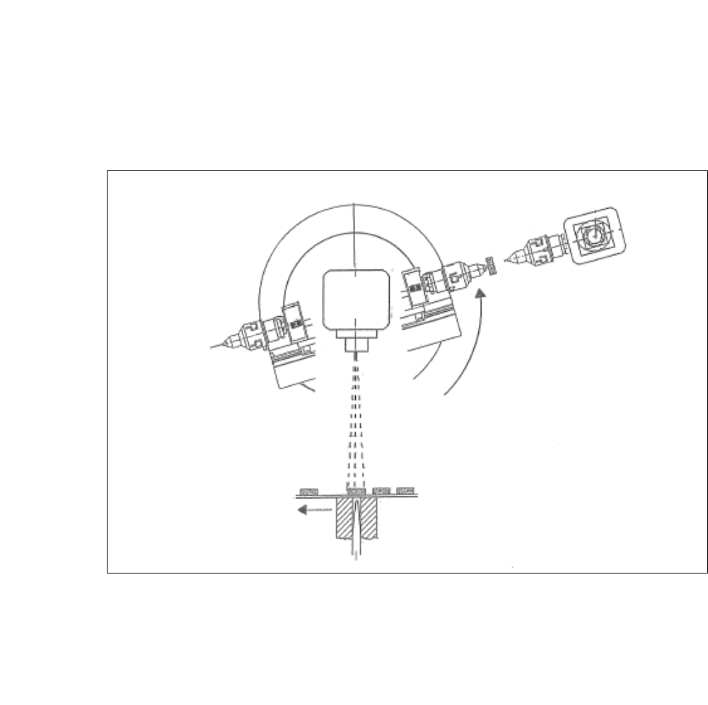
4.1.5.1 Flip Chip Segment 1 (Nozzle)
4
Fig. 4.1 - 6 Flip Chip Segment 1 (Nozzle)
(1) The wafer X-Y travels to the next chip
(2) The flip chip rotary unit segment 1 turns to the handover position "Die Attach".
During the rotation (from the camera "free Position") the picture recognition of the next chip
is carried out. 4
Wafer
Camera
4 SIPLACE Wafer System (SWS) User Manual SIPLACE CA-Series
4.1 Functions From software version SC.708.0 Edition 12/2014
208
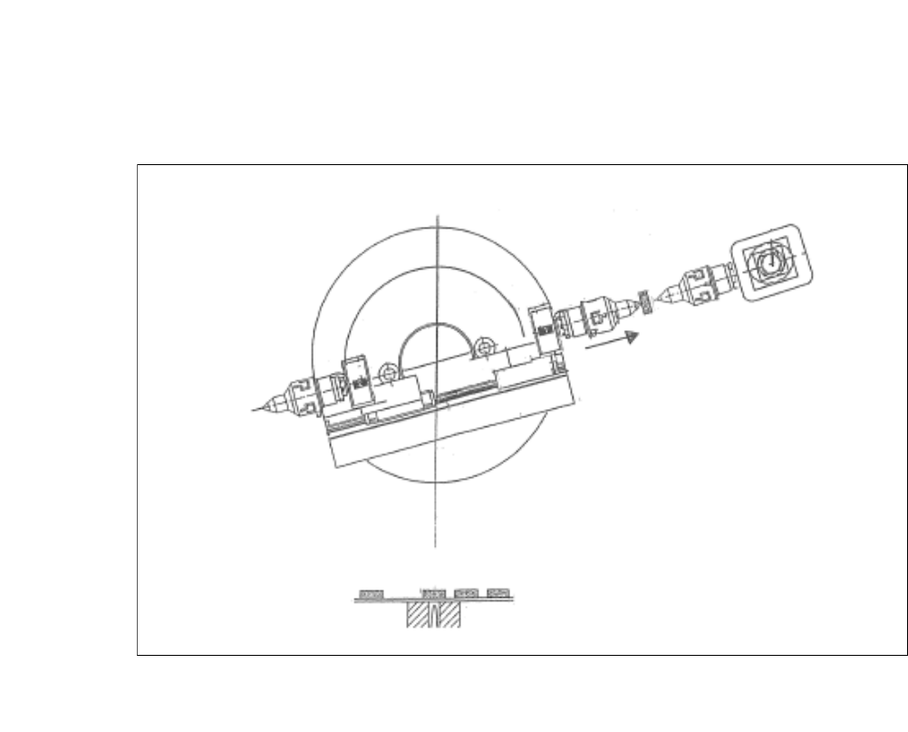
4.1.5.2 Flip Chip Segment 1 (Z Direction)
4
Fig. 4.1 - 7 Flip Chip Segment 1 (Z Direction)
(1) The x-axis of the flip chip swivel segment 1 is moved to the transfer position.