00197498-03_UM_SiplaceCA-Serie_EN.pdf - 第218页
4 SIPLACE Wafer System (SWS) User Manual SIPLACE CA- Series 4.3 Description of the SWS Modules From software version SC.708.0 Edition 12/2014 218 4 Fig. 4.3 - 3 Flip head - view from front (1) Nozz le take-up, seg ment 1…
User Manual SIPLACE CA-Series 4 SIPLACE Wafer System (SWS)
From software version SC.708.0 Edition 12/2014 4.3 Description of the SWS Modules
217
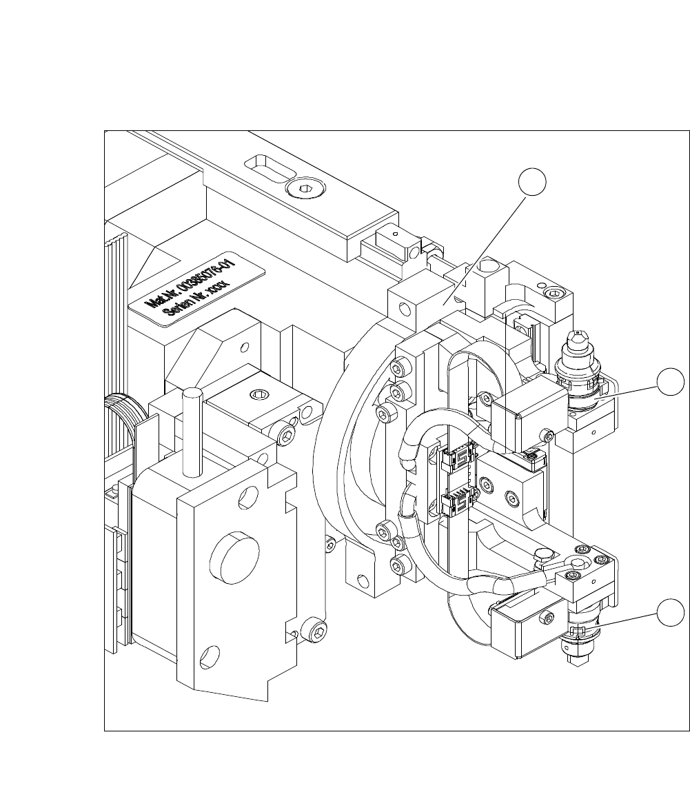
4.3.2 Flip Unit
4
Fig. 4.3 - 2 Flip Unit
4
4
(1) Flip head (2) Nozzle or tool take-up
1
2
2
4 SIPLACE Wafer System (SWS) User Manual SIPLACE CA-Series
4.3 Description of the SWS Modules From software version SC.708.0 Edition 12/2014
218
4
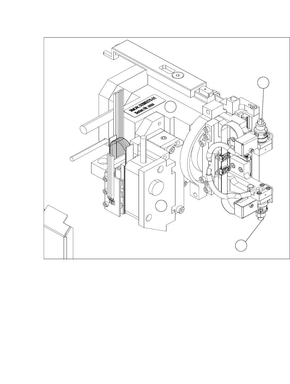
Fig. 4.3 - 3 Flip head - view from front
(1) Nozzle take-up, segment 1
(2) Nozzle take-up, segment 2
(3) Motor for linear movement
(4) Motor for 180° rotation
The flip unit takes the ejected die from the wafer foil. In flip chip mode, it rotates the die by 180°
into the pickup position for the placement head. In die attach mode, the flip unit rotates the die by
approx. 130° into the transfer position for the die attach unit.
The flip unit has two nozzles arranged at 180° to one another. This enables the system in flip chip
mode to pick up a new die from the wafer at the same time as the placement head performs
pickup.
The flip unit can use both the standard SIPLACE nozzles (9xx) and the special adapters for the
die bonding tool. As in the case of other SIPLACE placement machines, the dies are attached to
the nozzles by a vacuum.
1
3
4
2

User Manual SIPLACE CA-Series 4 SIPLACE Wafer System (SWS)
From software version SC.708.0 Edition 12/2014 4.3 Description of the SWS Modules
219
The flip unit has a rotation axis and a Z axis, driven by a linear motor. In the optional die attach
mode, a further linear motor transfers the dies to the die attach head. The rotary axis is responsible
for the rotation into the 180° position (flip chip mode) or 130° position (die attach mode). The Z-
axis moves the segment during the pick process. The optional linear motor in the die attach mode
moves the segment for transfer of the die to the die attach head.
4.3.3 Wafer Camera System
The wafer camera is aligned to the wafer surface. The camera image is used by the Vision system
to recognize the defined pattern for the die to be placed (also known as reference die), for ink spot
recognition (for operation without wafer map), calculation of the die position and for wafer edge
recognition. After positioning the wafer on the next die to be ejected, the Vision model is checked
and the die position determined. If the deviation from the target value is too great (tolerance can
be defined) the wafer table will be repositioned to optimize the ejection position.
Wafer edge recognition is needed to compensate any deviation of the wafer position relative to
the wafer frame, between different wafers of the same type.
Specification for standard camera system
The standard camera system is used for dies of size 1 to 12 mm.
The camera's field of vision is around 10.5 x 6.7 mm.
Specification high-resolution camera system
The high resolution camera system is part of the small die kit and is used for dies which are under
1 mm in size.
The camera's field of vision is around 16.0 x 12.8 mm.
4.3.4 Wafer Table
The wafer table consists of an X-Y unit (movement system with 2 linear axes) and the wafer sup-
port.
The wafer table moves the wafer support with the wafer to the required positions in the processing
area.