00197498-03_UM_SiplaceCA-Serie_EN.pdf - 第233页
User Manual SIPLACE CA-Series 4 SIPLACE Wafer System (SWS) From software version SC.708.0 Edition 12/20 14 4.4 Optional Components 233 4.4.3 Small Die Kit The small die kit is used if you need to process di es which are …
4 SIPLACE Wafer System (SWS) User Manual SIPLACE CA-Series
4.4 Optional Components From software version SC.708.0 Edition 12/2014
232
4.4.2 Die Attach Unit
4
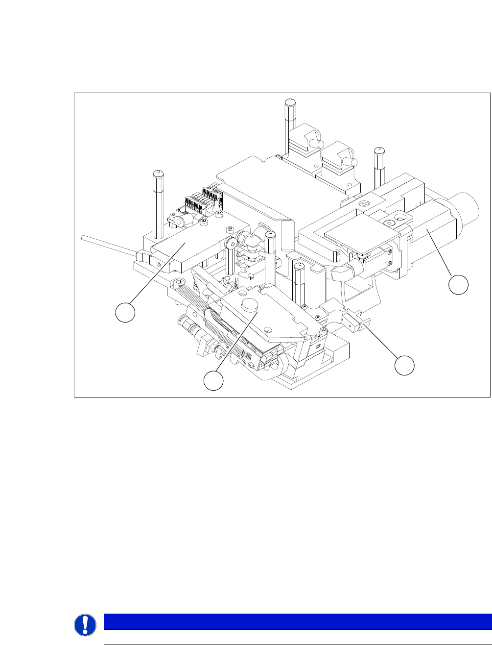
Fig. 4.4 - 2 Die Attach Unit
(1) Motor for rotating the die attach unit
(2) Driver
(3) Motor transfer X axis
(4) Solenoid valve
The die attach unit is needed for die attach mode.
The flip unit transfers the die to the die attach unit. The die is then rotated accordingly there and
made available for pickup. The die is therefore made available to the placement head in the same
top/bottom orientation as it was on the wafer and is placed in this position.
In die attach mode, only one of the nozzles for the flip unit functions. The flip unit takes up the next
die, while the current die is being picked up by the placement head from the die attach unit.
4
PLEASE NOTE
Do not use the die attach unit together with the LDU.
1
2
3
4

User Manual SIPLACE CA-Series 4 SIPLACE Wafer System (SWS)
From software version SC.708.0 Edition 12/2014 4.4 Optional Components
233
4.4.3 Small Die Kit
The small die kit is used if you need to process dies which are smaller than 1 mm. This kit is avail-
able on request as an option and consists of the following parts:
– A high-resolution camera system
– A small die ejector tool
– A component sensor
4.4.4 Wafer Map System
Wafer mapping is increasingly becoming a standard in die placement processes. The wafer map
assigns a function class to each die on the wafer.
The function class could simply be "good" or "bad". However, up to 255 classes can be assigned
to describe the die properties in detail.
Firstly, the SWS needs to identify the wafer. Normally, this involves reading in the barcode on the
wafer frame. This wafer ID is then used to select the required wafer file on the wafer map server.
In a second step, the abstract die ID from the wafer map file (column/row) is set in relation to the
real position of the die on the wafer. This position can be calculated by identifying special refer-
ence dies on the wafer and by determining the wafer center.
4
The wafer map function is primarily a software option. This includes a server system for the wafer
map files, with a conversion from customer-specific wafer map standard to the SWS standard.
4.4.5 Barcode Scanner
The barcode scanner on the SWS reads the barcode on the wafer frame.
PLEASE NOTE
Position calculation
The calculation of positions with the help of the wafer edge recognition function only
works reliably for dies which are 3 mm or larger.
4 SIPLACE Wafer System (SWS) User Manual SIPLACE CA-Series
4.4 Optional Components From software version SC.708.0 Edition 12/2014
234
4
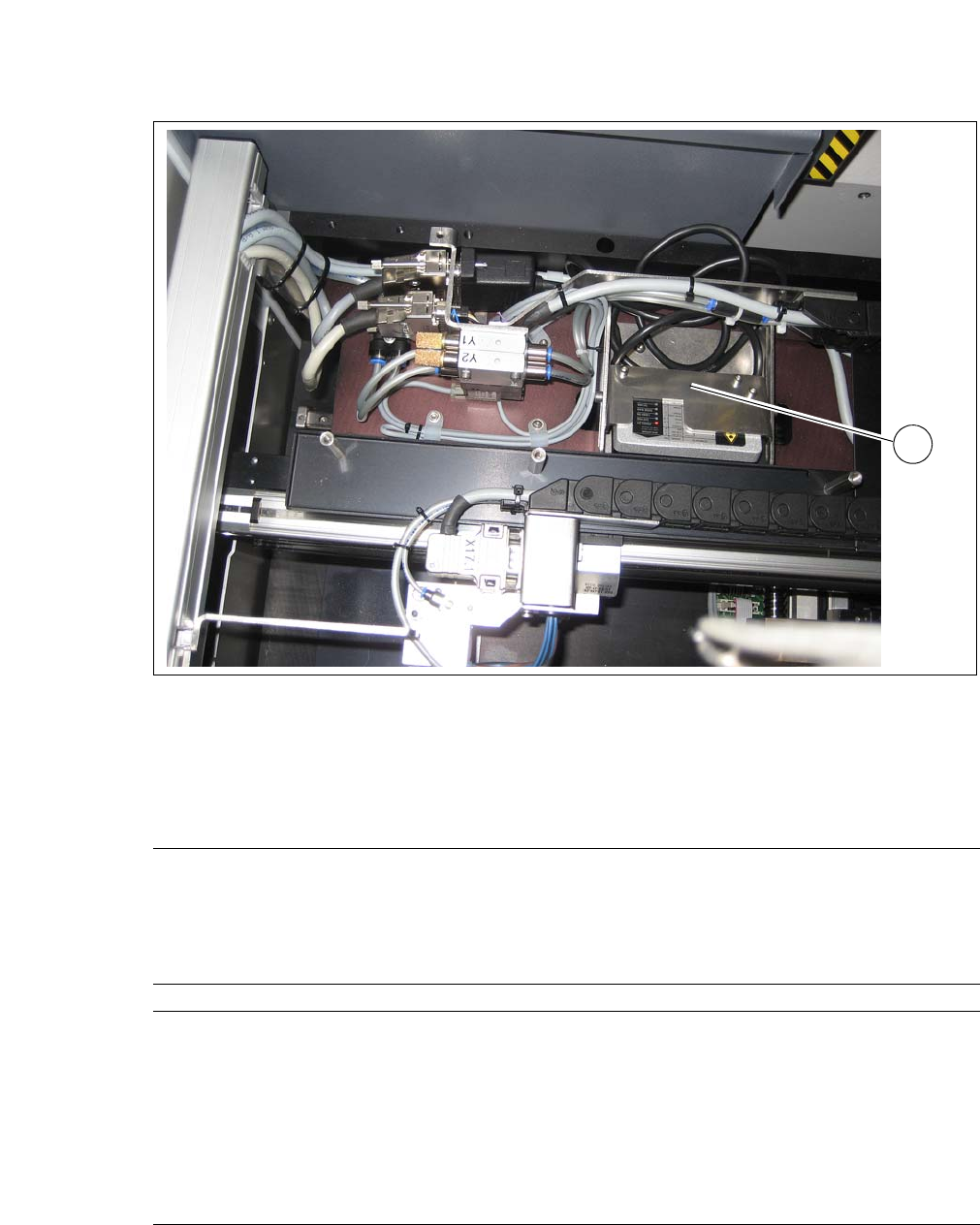
Fig. 4.4 - 3 Barcode scanner - installation example in the wafer changer
(1) Barcode Scanner
4.4.5.1 Technical Data
1
Board size
Length 50 mm to 610 mm
Width 50 mm to 508 mm
Thickness 0.3 mm to 4.5 mm
Curvature Up to 0.5 mm
Board types PCB, FR4, BGA, Boat, Leadframe
SIPLACE Wafer System
Placement method Flip chip, die attach
Die size 0.8 mm x 0.8mm up to 12 x12 mm
(larger dies on request)
Die thickness 0.05 mm to 4 mm
Wafer size Up to 12"
Frame size up to 15"
Wafer cassette max. 25 slots