3OM-1751-002w_G5S.pdf - 第173页
3OM-1751 2-5 1303-001 2.1.1 "Support pin up/dn" T ab Sheet [1] F3B4 [1] BL [mm] BR [mm] This is the offset data for the origin position of the support pin up/down axis which ascends or descends during PCB posit…
3OM-1751
2-41303-001
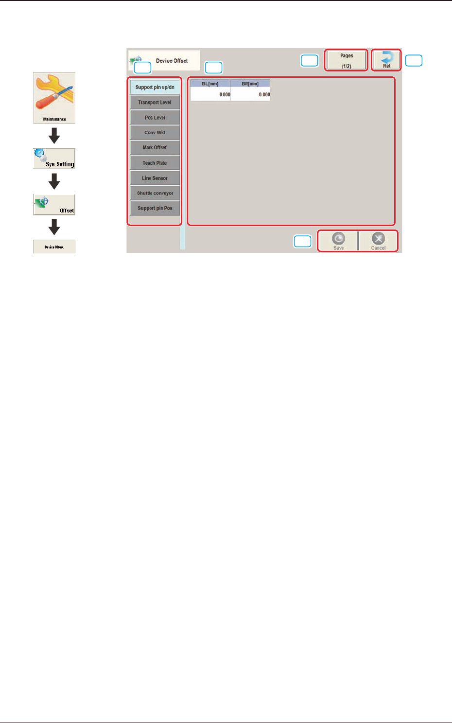
2.1 "Device Offset" Window
[1] [2]
[3]
[5]
[4]
F3B3
[1] Offset Select Tab
When this button is pressed, the offset data for the selected tab is displayed.
[2] Offset Data Display Section
In this section, the offset data selected in step [1] is displayed.
[3] Page Change Button
Using this button, the offset editing page is changed.
[4] [Ret] button
When this button is pressed, the "Offset Data" window is returned.
[5] [Save] button
When this button is pressed, the input data is saved.
[Cancel] button
When this button is pressed, the input data is cancelled and the save data is
returned.
Graphic
Development
2.1 "Device Offset" Window
3OM-1751
2-51303-001
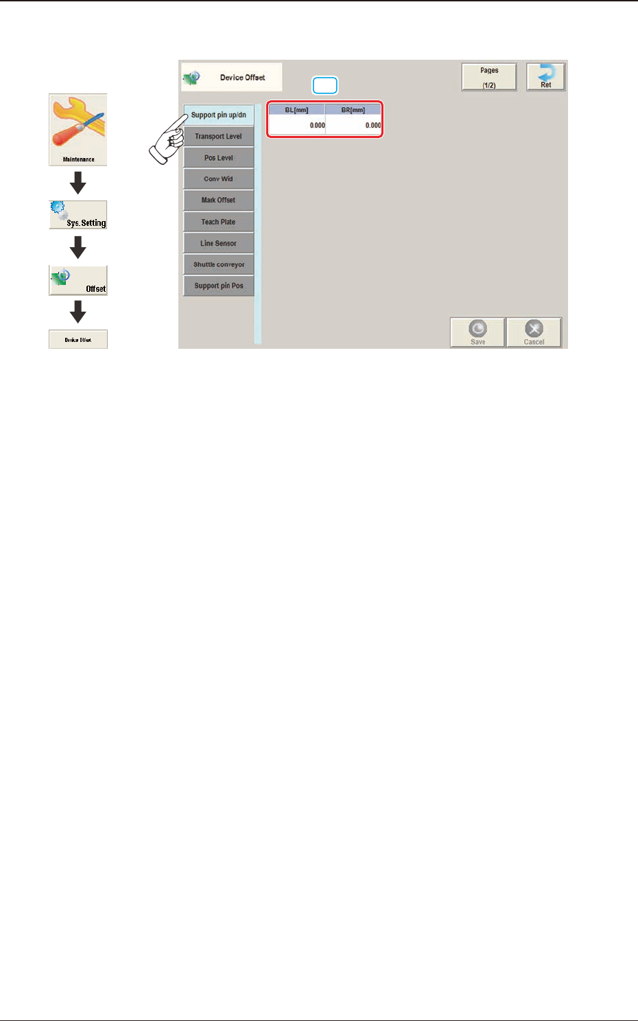
2.1.1 "Support pin up/dn" Tab Sheet
[1]
F3B4
[1] BL [mm]
BR [mm]
This is the offset data for the origin position of the support pin up/down axis
which ascends or descends during PCB positioning.
A plus (+) value decreases the ascending stroke during PCB positioning.
Graphic
Development
2.1 "Device Offset" Window
3OM-1751
2-61303-001
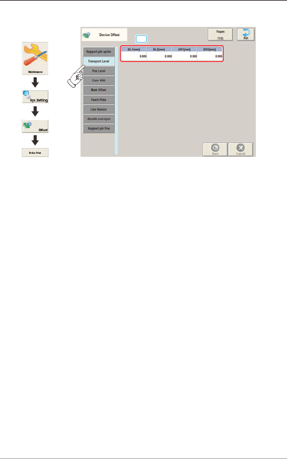
2.1.2 "Transport Level" Tab Sheet
[1]
F3B5
[1] BL1 [mm]
BL2 [mm]
BR1 [mm]
BR2 [mm]
Each parameters are used to correct the positional deviations in PCB transfer
positioning in comparison with Support pin up/down operation.
Graphic
Development
2.1 "Device Offset" Window