Siplace TX-设备参数-EN - 第24页
24 SIPLACE Vision High placement performance and best quality Board (substrate) recognition In addition to the precise recognition of componen ts, the PCB camera also guarantees r eliable detec- tion of inkspots and PCB …

23
SIPLACE Vision
High Placement Performance and Best Quality
SIPLACE Vision is designed
to recognize and measure
components and boards
(substrates), so that these
can then be placed and con-
nected precisely.
In the placement area,
SIPLACE Vision determines
the position of the compo-
nent on the nozzle and there-
fore facilitates exact
positioning of components
on the printed circuit boards.
There is a large component
library available which
already contains all standard
component shapes. Wizard
assistants, such as the Com-
ponent Shape Wizard, make
it easier to create new com-
ponent shapes.
Component recognition
SIPLACE Vision identifies each individual component by its geometry and color. Even complex com-
ponent shapes are detected with high reliability. This component recognition check is performed in a
single step, with no extra time involved but with optimum scanning of each individual component. The
camera types are adjusted to the various head types and present a range of different resolutions, field
of vision sizes, illumination types and focal areas. See also the technical data for the relevant place-
ment heads from page 9 onwards. With the help of different illumination levels and brightness stages,
almost every component shape can be easily recognized. The system also saves images of the com-
ponents, so-called "Vision dumps". These enable you to analyze rejected components and to further
improve component shape descriptions. This supports the early recognition of faults in new products
and increases process reliability. These vision dumps also serve as evidence in the event of defective
component supplies.
Component recognition is used for:
• Tolerance checks for component dimensions, L x W, (shape)
• Tolerance checks for component features e.g.:
• Lead/ball grids
• Lead/ball length/diameter
• Deformed leads/missing balls
• Damage/discoloration
• Flipped/face down
• Vision dumps in the event of malfunctions
• Pin 1 / polarity recognition
• Pattern matching
• Glue dot inspection
• Reading component barcodes/data matrix codes
• Pickup reliability
• Pocket measurement
• Tray measurement
• Offset of component to nozzle center and dynamic correction of pickup position

24
SIPLACE Vision
High placement performance and best quality
Board (substrate) recognition
In addition to the precise recognition of components, the PCB camera also guarantees reliable detec-
tion of inkspots and PCB fiducials.
Board recognition is used for:
• Position of fiducials for position recognition purposes
• Correction of elongation/compression
• Inkspot recognition
• Reading barcodes and data matrix codes
Nozzle measurement
• Type verification
• Nozzle concentricity
• Nozzle scan for contamination and wear
SmartPin Support
• Measurement of Smart Pins and their positions, plus constant monitoring during ongoing operations
Optional functions
• Teaching and recognizing OSC-THT (OSC package) see page 31.
• SIPLACE Vision teaching station
Separately from ongoing production, the SIPLACE Vision Teaching Station facilitates quick and
easy offline generation of component shape descriptions, even for complex components.
25
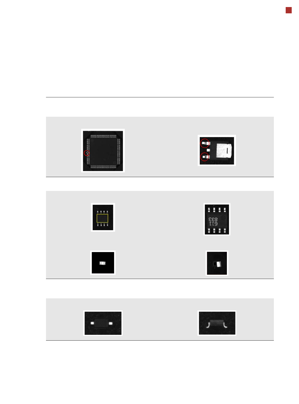
SIPLACE Vision
Component recognition
Checking the component quality
Recognizing the collinearity of components
Damaged or bent leads are recognized. This helps avoid solder-free connections during the subsequent solder-
ing process.
Damaged leads Damaged leads
Recognizing flipped (face down) or upright components
Both chip and IC component shapes (e.g. SOT) recognized in flipped (turned face down) or upright state.
SOT OK SOT “face down”
Flipped chip Chip upright
Checking the lead width
The optical checking of the lead width recognizes tilted or damaged leads. This helps to recognize e.g. diodes
with tilted leads.
Lead width OK Tilted lead