M20_Ope_E - 第206页
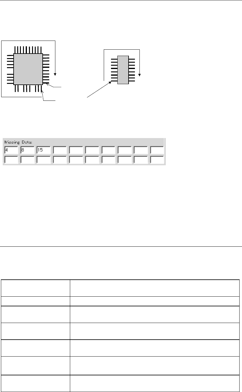
Chapter 5 Libraries 5-56 5-1-5-7 Missing Leads Assignment When the component has missing leads, click View >MissingData to open the View dialog box. Then enter missing lead numbers to the Mi ssing Data fields. As show…
Chapter 5 Libraries
5-55
5-1-5-6 Dimensions Settings and Others
Common Settings
z Dimensions Settings
Enter dimensions-related data of the scan target. When placing a cursor at a setting field, an
explanatory graphic for the setting and its description are displayed in sub-windows.
Note: An item displayed in yellow suggests its setting is out of the valid range.
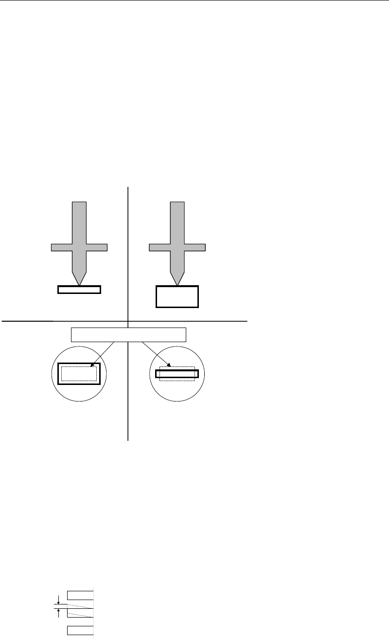
z Size Permission (1-100%)
The permission applied to the body size. Smaller the setting is, more severe the requirement
will be. Normally, specify 20% at "Size Perm." Set 30% at "Size Perm." for chip components with
the shorter side of less than 2.0mm, such as 1005 chip and 1608 chip. If the size of a component
is considerably irregular, use 40%.
Tilt placement: Permission
limit is exceeded.
Î
Retry
Normal placement
Bottom view
Side view
Nozzle
Minimum permission limit (dotted line)
z Offset Permission (1-100%)
The permission applied to the pickup position relative to the nozzle center. The default value
of 10% is set at "Offset Perm." for SOP, SOJ, PLCC, LCC, and QFP. If the offset is large, increase
this value.
z Lead Bend Permission
The permission applied to the horizontal lead bending.
Note: Default values are entered at Offset Permission and Lead Bend Permission in advance.
Chapter 5 Libraries
5-56
5-1-5-7 Missing Leads Assignment
When the component has missing leads, click View>MissingData to open the View dialog box.
Then enter missing lead numbers to the Missing Data fields. As shown in the below
illustrations, leads are numbered clockwise. (Numbering is performed based on the monitored
component image.) The result of your entry is graphically shown in the View dialog box.
The first lead
(
No.1
)
The last lead
Example 1 Example 2
The missing lead setting for Example 1 shall be as shown below (you can enter settings in any
order):
When you finish entering for a field, press <TAB> key to move to the next field.
The graphic shown in the View dialog box reflects the settings of the mold size, overall size,
lead count, lead width, and lead pitch, providing a good overview of the current settings.
Settings for Chip, Blob process, CPL process, Connector, BGA, and BGA/CSP are respectively
described in the following sections.
5-1-5-8 Chip Components
In the Image Data dialog box of Chip, select a component type by clicking <Mode> button.
Available component types are as followings. (Refer to the “Details of Vision Processing
Modes” for the details of each mode.)
Edge-midpoint Search
For older version data which uses this mode for standard chip
recognition (Re-processed by CPL in case of an image error).
Corner Search Used for components that can be recognized at corners only.
Overall Chip Process
Used for special components which cannot be processed by CPL.
This process time takes longer for heavy loading
.
Electrolytic Capacitor
Used for components with two reflective electrodes at the ends,
such as electrolytic capacitor.
CPL
Used for standard chip components. (This mode is normally
used.)
Edge-midpoint Search
(Non Recovery)
Normal Edge-midpoint Search mode without re-process by CPL.
Glass Melf
Used for cylindrical-shape-glass-encapsulated components with
two reflective electrodes at the ends

Chapter 5 Libraries
5-57
5-1-5-9 Blob Process
Blob Horizontal / Blob Vertical
White blobs with sizes more than "Blob X" and "Blob Y" are recognized as electrodes. In view of
allowance, enter 1/4 to 1/2 electrode size for "Blob X" and "Blob Y". Noises which come under
the size can be neglected.
Blob Area
Larger than the white blobs entered in “Blob area” are recognized as electrodes.
If you do not etner the blob area, approx. one-eighth area calculated from Overall XY and will
be automatically entered in “Blob area”.
Result of Image Processing (Display of the monitor screen)
Blob size: White blob dimensions are recognized as electrodes.
Detected areas are displayed in descending order as; [0], [1], [2]….
Area: The area white blobs are recognized as electrodes. (Unit: 0.01mm
2
)
Expert Sqr Size: Diagonal length of the rectangle defined by outer XY sides of white
blobs entered in Image Library edit window.
Actual Size : Actual measurement diagonal length of the rectangle defined by
outer XY sides of white blobs.
5-1-5-10 CPL Process
1
Normally, specify zero at “Prov.Position.” You can change the size and position of the
provisional positioning window.
Normally, specify zero at “Min Detect Size.” When a value is set to “Min Detect Size,” the
system recognizes an image having the Min Detect Size or longer length and ignores an image
having shorter length than the Min Detect Size.
5-1-5-11 Connectors
Applicable Component Styles
One-side leaded connector: With two or more leads. Only the leads reflect light. Center-leadless
lead row or center-molded lead row (see the below figure) can also be handled.
Two-side leaded connector: With two or more leads per side (4 or more in total). Only the leads
reflect light. Center-leadless lead rows or center-molded lead rows can also be handled
provided the opposing lead rows are symmetrical; if not symmetrical, the connector must be
handled with the one-side leaded mode.
Note: A Component with leads staggered both sides is applicable.
1
CPL: Coarse Part Location (Provisional Positioning)