M20_Ope_E - 第73页
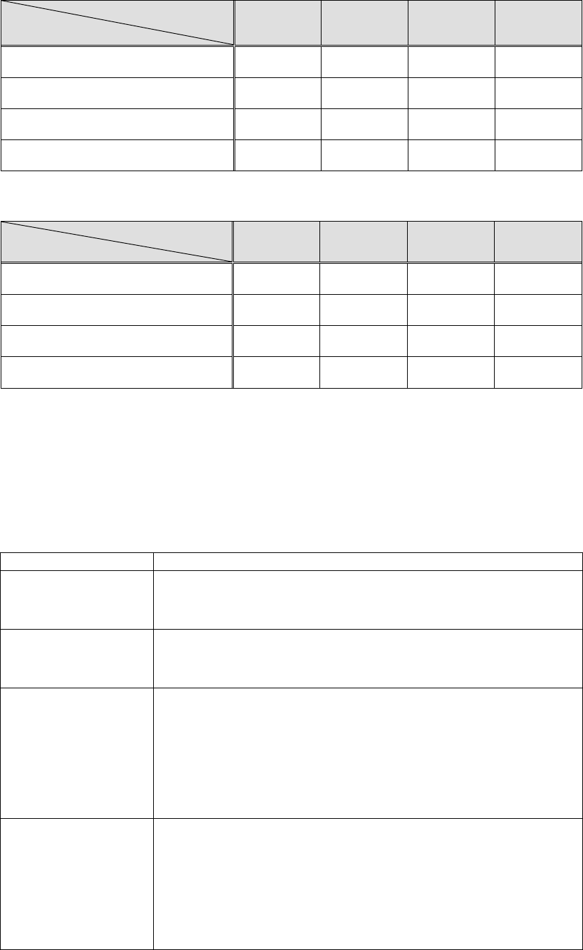
Chapter 2 Creating and Editing a Program 2-29 Anticipate transfer mode If [Loading next board after passed arrival sensor] is checked on, the anticipate transfer mode will be activated and the transfer time will be sho…
Chapter 2 Creating and Editing a Program
2-28
Normal transfer mode ([Loading next board after passed arrival sensor] is not checked on.)
Conveyor configuration
Time setting
Main
Entrance &
Main
Main & Exit
Entrance &
Main & Exit
Transfer time after PCB passed the
arrival sensor
X (Not
effective)
X (Not
effective)
X (Not
effective)
X (Not
effective)
Conveyor Run Time after Transfer Time
in Board Data
X (Not
effective)
X (Not
effective)
X (Not
effective)
X (Not
effective)
Delay for PCB Simul. Transfer
X (Not
effective)
X (Not
effective)
X (Not
effective)
X (Not
effective)
Transfer time after PCB passed the exit
sensor
○(Effective)
○(Effective)
○(Effective) ○(Effective)
Anticipate transfer ([Loading next board after passed arrival sensor] is checked on.)
Conveyor configuration
Time setting
Main
Entrance &
Main
Main & Exit
Entrance &
Main & Exit
Transfer time after PCB passed the
arrival sensor
○ (Effective)
○ (Effective)
○ (Effective) ○ (Effective)
Conveyor Run Time after Transfer
Time in Board Data
X (Not
effective)
○ (Effective)
X (Not
effective)
X (Not
effective)
Delay for PCB Simul. Transfer
X (Not
effective)
X (Not
effective)
X (Not
effective)
X (Not
effective)
Transfer time after PCB passed the exit
sensor
X (Not
effective)
X (Not
effective)
○(Effective) ○(Effective)
④ Detailed description of transfer mode
Normal transfer mode
If [Loading next board after passed arrival sensor] is not checked on, the normal transfer mode
will be activated.
The next board is loaded at the timings shown in the table below. For the normal transfer mode,
only the “Transfer time after PCB passed the exit sensor” timing setting is effective and other
timing settings will not be effective.
Conveyor configuration Board loading timing
Main After a component-mounted PCB has passed the exit sensor and then it has
been transferred only for a period of time set in [Transfer time after PCB
passed the exit sensor], the PCB stopper will be turned ON and the next
PCB will be loaded from the previous process.
Entrance & Main
(with entrance buffer)
After a component-mounted PCB has passed the exit sensor and then it has
been transferred only for a period of time set in [Transfer time after PCB
passed the exit sensor], the PCB stopper will be turned ON and the next
PCB will be loaded from the entrance buffer.
Main & Exit
(with exit buffer)
When a component-mounted PCB makes the exit buffer sensor turns on, the
PCB stopper will be turned ON and the next PCB will be loaded from the
previous process.
If the request signal is received from the next process when a
component-mounted PCB waits on the main conveyor and exit buffer, the
component-mounted PCB on the exit conveyor passes the exit sensor, and
then it is transferred only for a period of time set in [Transfer time after PCB
passed the exit sensor]. After that, the component-mounted PCB on the
main conveyor is unloaded to the exit buffer.
Entrance & Main & Exit
(with entrance buffer &
exit buffer)
When a component-mounted PCB makes the exit buffer sensor turns on, the
PCB stopper will be turned ON and the next PCB will be loaded from the
entrance buffer.
If the request signal is received from the next process when a
component-mounted PCB waits on the main conveyor and exit buffer, the
component-mounted PCB on the exit conveyor passes the exit sensor, and
then it is transferred only for a period of time set in [Transfer time after PCB
passed the exit sensor]. After that, the component-mounted PCB on the
main conveyor is unloaded to the exit buffer.

Chapter 2 Creating and Editing a Program
2-29
Anticipate transfer mode
If [Loading next board after passed arrival sensor] is checked on, the anticipate transfer mode will
be activated and the transfer time will be shortend.
Conveyor
configuration
Transfer time after
PCB passed the
arrival sensor
Conveyor Run Time
after Transfer Time in
Board Data
Delay for
PCB
Simul.
Transfer
Transfer time after
PCB passed the exit
sensor
Main After a
component-mounted
PCB has passed the
arrival sensor, and
then it has been
transferred only for
this period of time,
the PCB stopper will
be turned ON and
the next PCB is
loaded from the
previous process.
Not effective Not
effective
Not effective
Entrance &
Main
(with entrance
buffer)
After a
component-mounted
PCB has passed the
arrival sensor, and
then it has been
transferred only for
this period of time,
the PCB stopper will
be turned ON and
the next PCB is
loaded from the
entrance buffer.
After the next PCB has
been clamped, the
unloading operation is
performed only for this
period of time to
securely unload the
component-mounted
PCB that has been
transferred.
Not
effective
Not effective
Main & Exit
(with exit
buffer)
After a
component-mounted
PCB has passed the
arrival sensor, and
then it has been
transferred only for
this period of time,
the PCB stopper will
be turned ON and
the next PCB is
loaded from the
previous process.
Not effective Not
effective
After a
component-mounted
PCB has passed the
exit sensor, and then
it has been
transferred only for
this period of time,
the
component-mounted
PCB on the main
conveyor is
unloaded to the exit
buffer.
Entrance &
Main & Exit
(with entrance
buffer & exit
buffer)
After a
component-mounted
PCB has passed the
arrival sensor, and
then it has been
transferred only for
this period of time,
the PCB stopper will
be turned ON and
the next PCB is
loaded from the
entrance buffer.
Not effective Not
effective
After a
component-mounted
PCB has passed the
exit sensor, and then
it has been
transferred only for
this period of time,
the
component-mounted
PCB on the main
conveyor is
unloaded to the exit
buffer.
As the “Transfer time after PCB passed the arrival sensor” is changed, the transfer time can be
shortened. However, be sure to enter a numeric value exceeding 100 ms. If you enter a value that is
100 ms or less, the value you have entered is returned to the default value. If this time is too short,
the stopper may turn ON immediately after the arrival sensor has been turned OFF, causing the
PCB to be pushed up. In addition, please note that “Transfer time after PCB passed the arrival
sensor” is the time originating from when the sensor is turned OFF in the case of boards with
holes.
Caution
Chapter 2 Creating and Editing a Program
2-30
If the exit conveyor is not installed (exit buffer is not available), the PCB unloading completion
check with the exit sensor is not performed. Therefore, if this time setting is improper, a
component-mounted PCB may not be unloaded completely. So, take great care to make each time
setting.
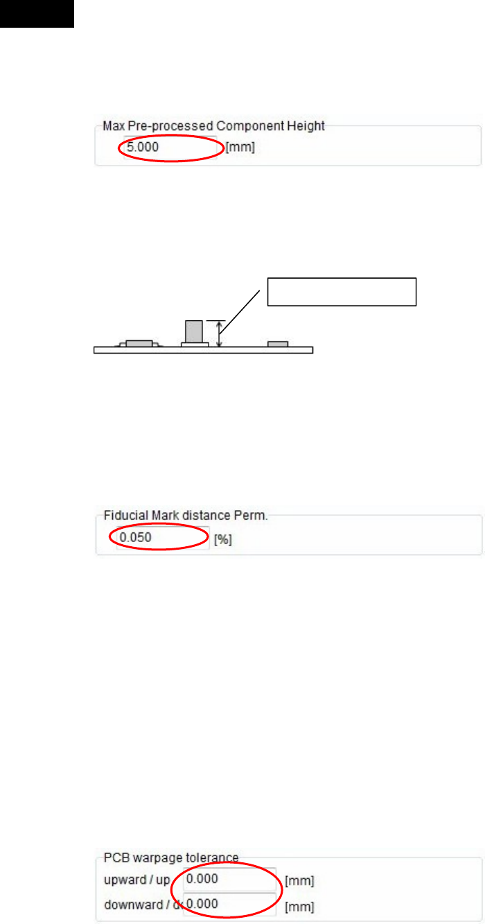
Max Pre-processed Component Height (Head travel height)
Enter the maximum component height already placed in the previous process.
First, the head travels over the PCB based on the setting, and then the head travel height is
adjusted based on the placed component height levels.
If there is no pre-processed component on the board, set “0.00”.
Fiducial Mark Distance Perm.
When the fiducial mark on the PCB is detected during production, the distance between the marks
is judged based on the distance between the marks of the fiducial mark coordinates set in the
program.
According to the results of this judgement, extended or contracted PCB or warped PCB can be
rejected without production.
Enter a permissible value (±%) in response to the reference distance value between the marks.
If the distance between the marks that have been detected exceeds this permissible value, relevant
error is given.
PCB warpage tolerance
Enter upward and downward PCB warpage tolerance values.
Tolerance values you can enter are 0 to 4.0 mm for the upward warpage tolerance and 0 to 1.0 mm
for the downward tolerance.
The force control is used in a range of “upward tolerance value + downward tolerance value” to
place components.
In particular, as you enter the downward warpage tolerance value, the placement height is made
low to take corrective actions against the PCB downward warpage.
Note: Basically, it is recommended to correct the PCB downward warpage using the push-up pin.
Caution
Max component height