M20_Ope_E - 第89页
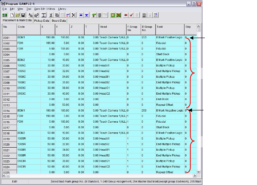
Chapter 2 Creating and Editing a Program 2-45 2-7-1-5 PCB Select Bad Mark This PCB select master bad mark function is design ed to select PCBs to be processed according to presence/absence of the bad mark on the PCBs. Us…
Chapter 2 Creating and Editing a Program
2-44
Bad Mark Positive/Negative Logic
Menu: Program>Placement&MarkData>Task>BMarkPositiveLogic
Program>Placement&MarkData>Task>BMarkNegativeLogic
The logic for bad mark skip operation is shown in the below table. This applies regardless of the
mark color.
Mark On Mark Off
B Mark Positive Logic Skip Place
B Mark Negative Logic Place Skip
Bad Mark Learning Feature
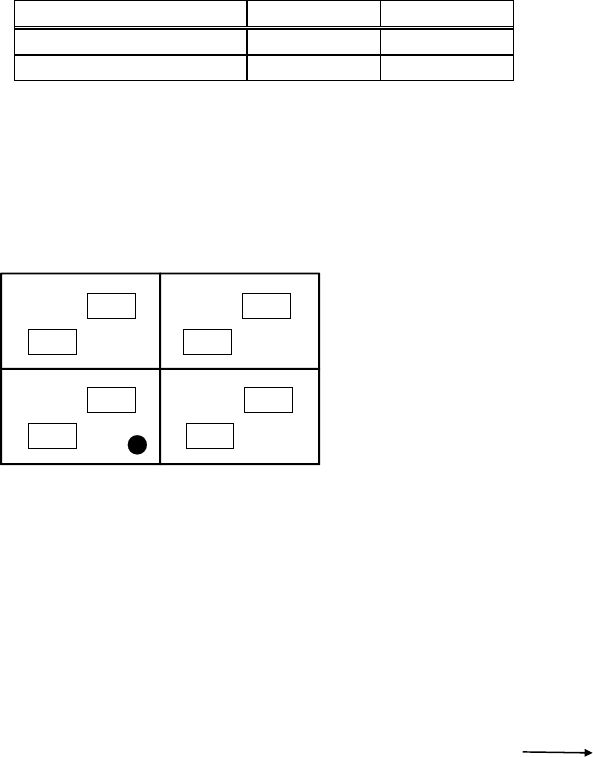
In running a repeat-block program including several bad mark steps with the same coordinates,
the system learns the result of the first bad mark process and applies it to the second or later bad
mark process. At this time, actual mark sensing is not performed and thus the cycle times can be
reduced. The following shows a typical example where this feature takes effect:
A
B
A
B
A
B
A
B
X Y Task
0.00 0.00 Start Block Placement
5.00 5.00 B Mark Positive Logic
: : (Placement routine A)
0.00 0.00 End Block Placement
60.00 0.00 Repeat Offset
60.00 40.00 Repeat Offset
0.00 40.00 Repeat Offset
0.00 0.00 Start Block Placement
5.00 5.00 B Mark Positive Logic
: : (Placement routine B)
0.00 0.00 End Block Placement
60.00 0.00 Repeat Offset
60.00 40.00 Repeat Offset
0.00 40.00 Repeat Offset
Note: This feature applies to up to 300 bad mark steps per program.
Bad mark process is
skipped.
Chapter 2 Creating and Editing a Program
2-45
2-7-1-5 PCB Select Bad Mark
This PCB select master bad mark function is designed to select PCBs to be processed according to
presence/absence of the bad mark on the PCBs. Use of this function allows programs to contain
multiple placement data. In other words, different types of PCBs can be processed on one
production line. This master bad mark is defined as bad mark No. #253. If this master bad mark is
not recognized, the program will execute data lines up to the line where the next PCB select bad
mark is specified.
Note: To use this function, the same PCB clamp setup condition must be set for every placement data. So
if the board size and reference hole position etc. differ from one PCB type to another, different
types of PCBs cannot be processed on the same production line.
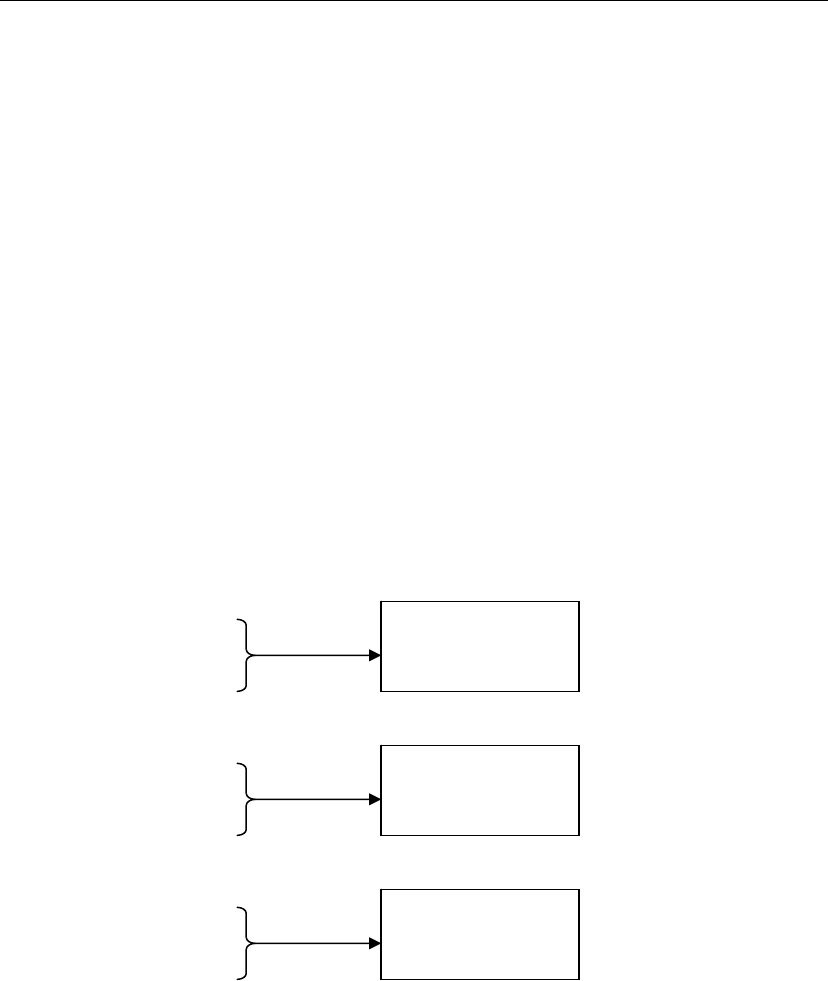
■PCB Select Bad mark Setting Method
① Add bad mark #253 as a master bad mark.
② If this PCB select master bad mark is not recognized, the program will execute data lines up
to the line where the next PCB select bad mark is specified.
PCB select bad mark A
(#253)
Placement data
:
PCB select bad mark B
(#253)
Placement data
:
PCB select bad mark C
(#253)
Placement data
:
Note: Since this PCB select master bad mark is not taken into account by offline software programs, it
must be programmed last on the mounter.
Board data for
board A
Board data for
board B
Board data for
board C
Chapter 2 Creating and Editing a Program
2-46
Note: When using the PCB select master bad mark function, the following must be observed.
① In principle, the “Preliminary Fiducial Process” and “Preliminary Bad Mark Process” user
parameters must be set to “Disable”. If they are set to “Enable”, the tact time will lengthen
since all the fiducial and bad marks on the program are processed first.
② Two or more PCB types of program data are defined in the program, but they are handled as
one type at program management.
③ The PCB select bad mark must be set using the mark coordinates by which only the target
PCB can be identified.
Note: As the example given in “PCB Select Bad mark Setting Method” in the previous page, in order to
identify more than three PCB types, the PCB select bad mark positions must differ from each other.
However, when identifying only two PCB types, the same coordinates can be used for the PCB
select bad marks by setting the positive/negative logic of the bad mark function as shown above.
In this case, recognition of the bad marks is performed only once, resulting in shorter tact time.
④ To use PCB select bad marks, block data conversion must have been performed on the
placement program for each PCB. If a repeat block is defined for each PCB type, the program
must be converted using the block data conversion function.
⑤ If any of the placement programs are not selected, a “#1548 No PCB has been selected in the
PCB select bad mark" process."” error will occur and the mounter stops. In this case, cancel
production and remove the board.
Note: Block Data Conversion Function
Data Edit Utilities> Block Data Conversion
Data for board 2
PCB select
master bad mark
for board 2
Data for board 1
PCB select
master bad mark
for board 1