IPC-4556 印制板化学镍钯浸金(ENEPIG)规范ENG.pdf - 第16页
3.1.1 High Magnification Reference Images It may be necessary to evaluate the ENEPIG deposit using scanning electron microscopy (SEM), transmission electron microscopy (TEM) or focused ion beam (FIB) as part of a qualific…
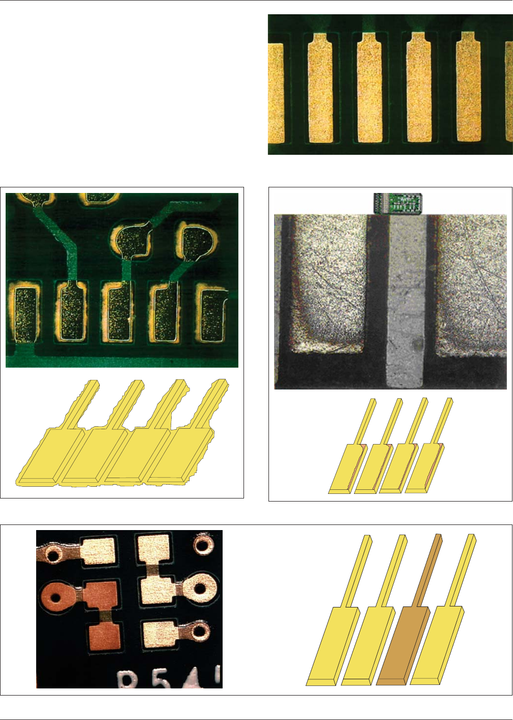
3.1 Visual ENEPIG surfaces shall be inspected in accor-
dance with the visual examination sections of the IPC-6010
series specifications, specifically IPC-6012 which specifies the
use of a nominal magnification of 1.75X (approx. 3 diopters).
The coverage shall be complete and the finish shall be uni-
form on the surfaces to be plated (see Figure 3-1). For higher
magnification analysis, Figures 3-2 to 3-4 are offered for ref-
erence purposes. There shall be no extraneous plating or
nickel foot (see Figure 3-2), edge pull back (see Figure 3-3) or
skip plating (see Figures 3-4, 3-5 and 3-6) on the surfaces of
all classes of product.
Figure 3-1 Uniform Plating
IPC-4556-3-2a/2b
Figure 3-2 Extraneous Plating or Nickel Foot
IPC-4556-3-3a/3b
Figure 3-3 Edge Pull Back
IPC-4556-3-4a/4b
Figure 3-4 Skip Plating
January 2013 IPC-4556
5
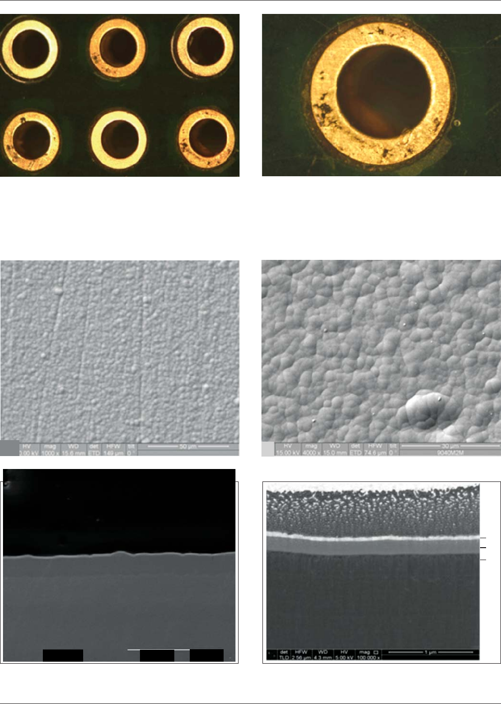
3.1.1 High Magnification Reference Images It may be necessary to evaluate the ENEPIG deposit using scanning electron
microscopy (SEM), transmission electron microscopy (TEM) or focused ion beam (FIB) as part of a qualification plan and
or for failure analysis. The images in Figures 3-7 through 3-12 in the following section are for reference purposes and were
provided by several different suppliers of ENEPIG.
Figure 3-5 Skip Plating of Gold Over Palladium Figure 3-6 Skip Plating of Gold Over a Palladium Deposit
Figure 3-7 1000X SEM Image of a Normal ENEPIG Surface Figure 3-8 4000X SEM Image of a Normal ENEPIG Surface
Figure 3-9 2500X FIB Image of a Normal ENEPIG Deposit Figure 3-10 100,000X FIB Image of a Normal ENEPIG
Deposit
Au
Pd
Ni
IPC-4556 January 2013
6
×2.5k
20kV
20 m
察
察
3.2 Finish Thickness Thicknesses of the electroless nickel,
electroless palladium and immersion gold layers shall be mea-
sured and verified following the completion of the ENEPIG
plating operation in the printed board fabrication process. The
use of X-ray fluorescence (XRF) methodology for thickness
determination shall be in accordance with APPENDICES 4
and 9 of this document and shall employ XRF instrumentation
equipped with software and hardware appropriate for ENEPIG
measurement. The committee has performed extensive round
robin testing of equipment capability to accurately measure
this tertiary deposit (see APPENDICES 3, 9 and 10). The
results showed a number of critical issues with equipment,
set-up, measuring protocols and reference standards. It is
imperative to demonstrate measurement capability in order to
meet the following thickness specification.
3.2.1 Electroless Nickel Thickness The electroless nickel
thickness shall be 3 to 6 µm [118.1 to 236.2 µin] at ± 4 sigma
(standard deviations) from the mean as measured on a nominal pad size of 1.5 mm x 1.5 mm [0.060 in x 0.060 in] or equiva-
lent area, where standard feature size tolerances as expressed in the IPC-6010 standard series, apply. This upper end of this
thickness specification has been chosen based on concerns with insertion force issues for compliant pin applications ONLY.
Use of thicknesses outside of this range shall be AABUS.
3.2.2 Electroless Palladium Thickness The electroless palladium thickness shall be 0.05 to 0.30 µm [2 to 12 µin] at ± 4
sigma (standard deviations) from the mean as measured on a nominal pad size of 1.5 mm x 1.5 mm [0.060 in x 0.060 in] or
equivalent area, where standard feature size tolerances as expressed in the IPC-6010 standard series, apply. The upper thick-
ness limit may be exceeded to meet specific design criteria (for example, applications requiring wire bonding but no solder-
ing).
3.2.3 Immersion Gold Thickness The minimum immersion gold thickness shall be >0.030 µm [1.2 µin] at - 4 sigma
(standard deviations) below the mean as measured on a nominal pad size of 1.5 mm x 1.5 mm [0.060 in x 0.060 in] or
equivalent area, where standard feature size tolerances as expressed in the IPC-6010 standard series, apply. The specification
is one sided, based on performance test results showing impaired solderability performance after accelerated aging at lower
gold thicknesses. The nature of the reaction of immersion gold with electroless palladium is such that substantially greater
thicknesses may not be achievable.
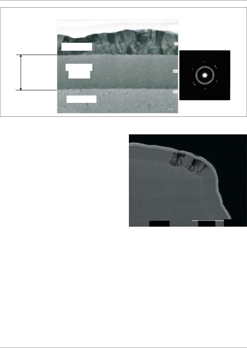
Figure 3-11 TEM Image of a Normal ENEPIG Deposit
[The Palladium-Phosphorus film is amorphous and very uniform whereas the gold (Au) deposit is crystalline in nature.]
Figure 3-12 2500X Image of Nickel that is Hyper-Corroded
(This is due to excessive dwell time in the gold bath.)
January 2013 IPC-4556
7
×2.5K
20kV
20 m
60 nm
TEM image
Au deposit
Palladium
deposit
EN deposit
推着额期
Electron diffraction of
Palladium film