IPC-4556 印制板化学镍钯浸金(ENEPIG)规范ENG.pdf - 第18页
Note: Some designs may not have feature sizes of this specified pad area and will require the use of alternate pad sizes. The XRF collimator used shall always be smaller than the pad used for measurement; and specifically …
3.2 Finish Thickness Thicknesses of the electroless nickel,
electroless palladium and immersion gold layers shall be mea-
sured and verified following the completion of the ENEPIG
plating operation in the printed board fabrication process. The
use of X-ray fluorescence (XRF) methodology for thickness
determination shall be in accordance with APPENDICES 4
and 9 of this document and shall employ XRF instrumentation
equipped with software and hardware appropriate for ENEPIG
measurement. The committee has performed extensive round
robin testing of equipment capability to accurately measure
this tertiary deposit (see APPENDICES 3, 9 and 10). The
results showed a number of critical issues with equipment,
set-up, measuring protocols and reference standards. It is
imperative to demonstrate measurement capability in order to
meet the following thickness specification.
3.2.1 Electroless Nickel Thickness The electroless nickel
thickness shall be 3 to 6 µm [118.1 to 236.2 µin] at ± 4 sigma
(standard deviations) from the mean as measured on a nominal pad size of 1.5 mm x 1.5 mm [0.060 in x 0.060 in] or equiva-
lent area, where standard feature size tolerances as expressed in the IPC-6010 standard series, apply. This upper end of this
thickness specification has been chosen based on concerns with insertion force issues for compliant pin applications ONLY.
Use of thicknesses outside of this range shall be AABUS.
3.2.2 Electroless Palladium Thickness The electroless palladium thickness shall be 0.05 to 0.30 µm [2 to 12 µin] at ± 4
sigma (standard deviations) from the mean as measured on a nominal pad size of 1.5 mm x 1.5 mm [0.060 in x 0.060 in] or
equivalent area, where standard feature size tolerances as expressed in the IPC-6010 standard series, apply. The upper thick-
ness limit may be exceeded to meet specific design criteria (for example, applications requiring wire bonding but no solder-
ing).
3.2.3 Immersion Gold Thickness The minimum immersion gold thickness shall be >0.030 µm [1.2 µin] at - 4 sigma
(standard deviations) below the mean as measured on a nominal pad size of 1.5 mm x 1.5 mm [0.060 in x 0.060 in] or
equivalent area, where standard feature size tolerances as expressed in the IPC-6010 standard series, apply. The specification
is one sided, based on performance test results showing impaired solderability performance after accelerated aging at lower
gold thicknesses. The nature of the reaction of immersion gold with electroless palladium is such that substantially greater
thicknesses may not be achievable.
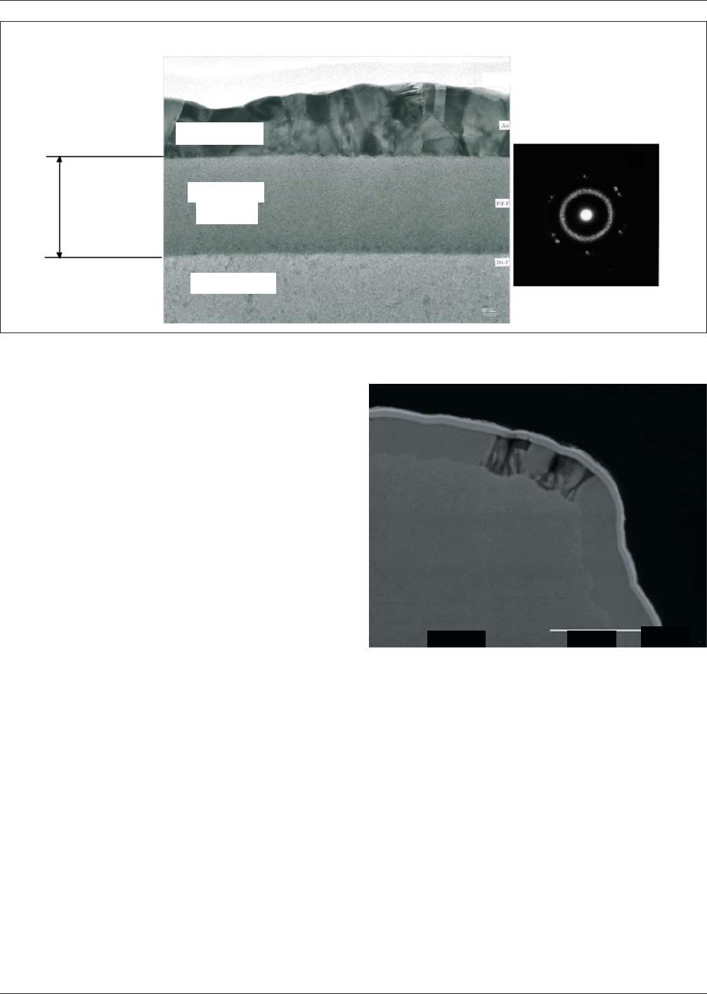
Figure 3-11 TEM Image of a Normal ENEPIG Deposit
[The Palladium-Phosphorus film is amorphous and very uniform whereas the gold (Au) deposit is crystalline in nature.]
Figure 3-12 2500X Image of Nickel that is Hyper-Corroded
(This is due to excessive dwell time in the gold bath.)
January 2013 IPC-4556
7
×2.5K
20kV
20 m
60 nm
TEM image
Au deposit
Palladium
deposit
EN deposit
推着额期
Electron diffraction of
Palladium film

Note: Some designs may not have feature sizes of this specified pad area and will require the use of alternate pad sizes. The
XRF collimator used shall always be smaller than the pad used for measurement; and specifically, the collimator shall not
exceed 30% of the feature pad size being measured. For smaller sized pads, the measurement time will need to increase
proportionately as a function of collimator area reduction. Consistency of the pad size used for measurement is of primary
concern in order to obtain a statistically valid result, due to the typical plating thickness variation seen as a function of pad
size. In general, smaller features will plate thicker than larger features. The use of fiducial pads for this measurement is sug-
gested for those designs not having the specified pad feature areas, described above.
3.2.4 XRF Calibration Standards The use of National Standards traceable calibration standards with similar thicknesses to
the specified ENEPIG thicknesses which are to be measured, is recommended. Tri-layer standards where Au and Pd are
plated directly on Ni/Cu/PCB should be used for calibration for Cu thicknesses >30 µm. Tri-layer foil standards where Au
and Pd are plated on a Ni-foil should be used if boards with varying Cu-thicknesses are to be measured. Additional infor-
mation can be found in Appendix 10.
For Cu thickness >30 µm, a combination of a minimum of two calibration standards with approximate thicknesses, as below,
should be used.
• Au/Pd/Ni/Base 0.05 µm/0.02 µm/3 µm/>30 µm
• Au/Pd/Ni/Base 0.05 µm/0.09 µm/3 µm/>30 µm
• Au/Pd/Ni/Base 0.05 µm/0.3 µm/3 µm/>30 µm
• Au/Pd/Ni/Base 0.1 µm/0.2 µm/3 µm/>30 µm
For Cu thicknesses <30 µm a combination of a minimum of two calibration foil standards with approximate thicknesses as
below, should be used.
• Au/Pd/Ni/Base 0.06 µm/0.02 µm/4 µm/<30 µm
• Au/Pd/Ni/Base 0.06 µm/0.06 µm/4 µm/<30 µm
• Au/Pd/Ni/Base 0.05 µm/0.1 µm/4 µm/<30 µm
• Au/Pd/Ni/Base 0.05 µm/0.25 µm/4 µm/<30 µm
For additional details, see APPENDICES 4 and 9.
3.2.5 Use of Non-Statistical Thickness Specification For production lot sizes of ten printed boards or less, i.e., proto-
type builds, the need to demonstrate compliance to the statistical requirements above are negated, provided that measure-
ments are taken on 100% of all printed boards/panel coupons, thus providing population parameters rather than sample sta-
tistics. All such readings shall fall within the thickness ranges specified above for all three deposits. Any readings below or
above the specified thickness range shall be cause for rejection of that board.
3.2.6 Production Overruns and/or Inventory Items When compliance testing of individual printed board(s) remaining in
inventory is required, use the protocol of 3.2.5. For production overruns larger than ten, the sample statistic constraints shall
apply.
3.3 Porosity An ENEPIG immersion gold layer is not totally impervious and is not able to pass the requirements of a
‘classic’ porosity test (for example, Nitric Acid per ASTM B 735).
3.4 Adhesion The purpose of adhesion testing for ENEPIG finished boards is twofold.
1) The primary purpose of the testing is to verify that there is no adhesion failure between the metallic layers of the fin-
ish, or the finish and the base metal. The tape testing shall be carried out in accordance with IPC-TM-650, Method
2.4.1, using a strip of pressure sensitive tape. There shall be no evidence of any portion of the surface finish being
removed, as shown by particles of plated deposit/pattern adhering to the tape. If soldermask overhang breaks off and
adheres to the tape, it is evidence of undercut but not of adhesion failure.
2) The secondary purpose is for testing the adhesion of the solder mask to both traces and laminate. Both the chemistry
used in the ENEPIG process and the required dwell times and temperatures can have a negative impact on solder mask
adhesion. – Note: Not all solder masks are compatible with an ENEPIG process.
In both cases, testing should be conducted on regions of high feature density on the board, such as BGA sites, dams between
fine pitch leaded devices or over areas of high trace density. Using the same approach as for the test for metal adhesion,
check for evidence of the soldermask being removed, as shown by particles of soldermask adhering to the tape.
IPC-4556 January 2013
8
Because of the requirement to test in high density areas, the potential to leave tape residue that could interfere with solder-
ing exists, especially if an incorrect type of tape is used. Verification of zero impact to solderability must be demonstrated
for the areas tested, or the area tested shall not be used for final product.
3.5 Solderability The thickness specification described herein shall meet the Category 3 coating durability requirements of
J-STD-003, i.e., greater than 12 months shelf life.
Note 1: The use of steam exposure (conditioning) is not an applicable accelerated stress test method for ENEPIG.
Note 2: While adherence to the IPC-1601 recommendations for baking prior to assembly may have a negative impact on
solderability performance, the requirements for solderability testing in this specification are for samples tested without bak-
ing. Any deviation from this shall be AABUS.
For details of the solder spread testing data from the round robin, see APPENDIX 6. Ball shear data from the same study is
documented in APPENDIX 7.
3.5.1 Force Measurement Testing (Wetting Balance Test-
ing)
The following requirements are based on the use of the
Standard IPC coupon, Figure 3-13, immersed to a depth of
0.6mm at 90 degrees incidence to the solder surface. The
dwell time shall be ten seconds. For details of the wetting bal-
ance data from the round robin study, see APPENDIX 5.
• Force measurement testing of an ‘‘as received’’ sample with
Eutectic SnPb solder, using the prescribed Test Flux#1at
235 °C, shall produce a positive wetting force within 2 sec-
onds and a minimum wetting force of 0.14 mN/mm.
• For force measurement testing of samples stressed for 8
hours @ 72 °C [162 °F] and 85% R.H, the increase in wet-
ting time shall not exceed 1 second. The wetting force shall
be a minimum of 0.12 mN/mm.
• For force measurement testing of ‘‘as received’’ samples with SAC305 solder, using the prescribed Test Flux#2at
255 °C, shall produce a positive wetting force within 1.5 seconds and a minimum wetting force of 0.19 mN/mm.
• For force measurement testing of samples stressed for 8 hours @ 72 °C [162 °F] and 85% R.H., the increase in wetting
time shall not exceed 1 second. The wetting force shall be a minimum of 0.17 mN/mm.
3.6 Cleanliness The surface of an ENEPIG finish is typically cleaner than most other surface finishes. Ionic cleanliness
shall be established per the requirements of IPC-5704, which specifies a sample size of 11. It is recommended that solvent
extract conductivity (SEC) testing per IPC-TM-650, Method 2.3.25, also be performed at the same time as the IPC-5704
qualification, to establish process control parameters. SIR testing shall be per IPC-TM-650, Method 2.6.3.5. The require-
ments for SIR test performance shall be as specified in Table 3-1. Failure to meet this cleanliness specification should trigger
immediate process control corrective action.
3.7 Electrolytic Corrosion The ENEPIG process contains chemistries that are ionic in nature, but which are readily rinse-
able. Both the quality and volume of water used for the rinsing steps between process baths, and for the final rinsing of the
product are critical if the potential for electrolytic corrosion is to be avoided. The use of IPC-TM-650, Method 2.6.14.1,
‘‘Electrochemical Migration Resistance Test’’ is recommended for high reliability applications, or for designs with high fea-
ture density. The resistance values shall not drop more than one order of magnitude after the test has been completed.
4 QUALITY ASSURANCE PROVISIONS
4.1 General Quality Assurance Provisions
These are specified in IPC-6011 and each IPC-60XX sectional specification.
Additional requirements for printed boards with electroless nickel/electroless palladium/immersion gold (ENEPIG) plating
are specified herein for qualification, acceptance, and quality conformance.
Figure 3-13 The Standard IPC Force Measurement
4.1.1 Qualification Recommendations Qualification of a printed board supplier, supplying ENEPIG to this specification
shall be AABUS (see IPC-6011). The process capability of a supplier of PWB with ENEPIG finish shall be established by
demonstrating process control over time. Table 4-1 provides a listing of suggested qualification elements that should be exer-
cised by the supplier. It includes the associated requirements and/or test methods when applicable.
Coupon
January 2013 IPC-4556
9