IPC-4556 印制板化学镍钯浸金(ENEPIG)规范ENG.pdf - 第50页
APPENDIX 6 Solder Spread Testing Brian Madsen Continental Automotive Systems Solder spread testing was performed on printed boards with seven dif ferent ENEPIG chemistries. Samples with a range of electroless palladium t…
Summary of Soldering ENEPIG Post 8 Hours of 72 °C/85% R.H Exposure:
1) The stressing protocol was able to differentiate ‘‘good’’ from ‘‘bad’’ ENEPIG deposits.
2) The test results were capable of defining a minimum gold thickness for the specification.
3) For the more robust ENEPIG deposits, the exposure to the stressing protocol had little impact on wetting times and final
wetting forces, however the time to reach the maximum force increased.
4) Stressing deposits that were already 8 months old had little impact on the ‘‘good’’ samples, whereas the ‘‘bad’’ samples
were significantly affected.
SUMMARY
The continuing use of the wetting balance by the 4-14 Committee to define acceptable deposit thickness and performance
characteristics was once again confirmed with this round of extensive testing. From this testing, a pass-fail criterion has
finally been established for the wetting balance testing of ENEPIG, which will also be included in the upcoming revision
of IPC J-STD-003C. Six sample groups of ENEPIG were evaluated and were found, in the majority of cases, to exhibit very
little difference in performance as a function of electroless palladium deposit thickness. However immersion gold thickness
was found to have a major impact on robustness and potentially shelf life. Differences were evident between the suppliers,
especially post stressing of the deposit. Each supplier was provided only with the identifier for their own ENEPIG sample(s),
allowing them to know the performance of their own process, but not of any specific competitor. It is hoped that the lower
performing groups use this information to improve their process performance, especially post stressing.
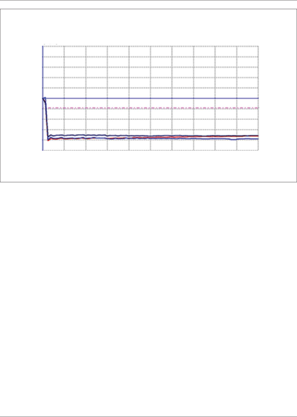
IPC-4556-a5-15
Figure A5-15 Performance of Sample Group 20 (with thin gold) with SAC305 Post Stressing
(Note: The performance was not improved even with the increased activity flux and higher temperature used for SAC305 testing).
Sample 20 0.56Au/4.77Pd/219.95Ni
post 8 hours 72C/85% R.H.
Fr(mN/mm)
Standard : NF-A-89 400P
t(s)
0.25
0.20
0.15
0.10
0.05
0.00
-0.05
-0.10
-0.15
-0.20
12345678910
-0.25
January 2013 IPC-4556
39
APPENDIX 6
Solder Spread Testing
Brian Madsen
Continental Automotive Systems
Solder spread testing was performed on printed boards with seven different ENEPIG chemistries. Samples with a range of
electroless palladium thickness (targeted thicknesses from 0.1 to 0.5 µm) were provided for each of the seven chemistries.
While the intention had been to evaluate 3 to 4 electroless palladium thicknesses per chemistry through four test conditions,
unfortunately a shortage of samples for some chemistries resulted in incomplete data sets (see Table A6-S1). Two solder
pastes were used to evaluate the solder spread on the ENEPIG deposits - a Sn/Pb/Ag eutectic alloy solder paste with flux
activity level ROL1 and a SAC300 family Pb-free paste with flux activity level ROL0. For each solder paste, one test board
was subjected to 8 hours of damp heat conditioning at 72 °C [162 °F] and 85% relative humidity prior to printing the sol-
der paste, while a second board was printed with no pre-conditioning. Each individual test board contained 16 solder spread
coupons (layout shown in Figure A6-S1).
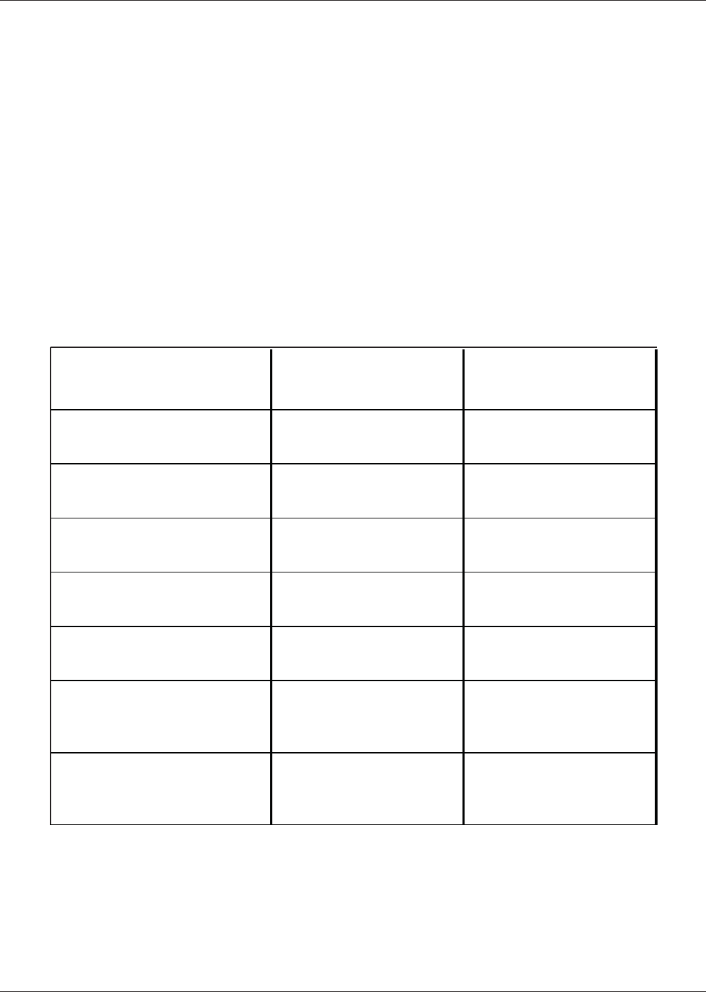
Table A6-S1 Preconditioning and Solder Paste Matrix Used for Solder Spread
Testing for a Given ENEPIG Chemistry and Electroless Palladium Thickness
(Note: When sufficient samples available)
None
8h 72° C/85%
None
8h 72° C/85%
0.1 µm X X X X
0.2 µm X X X X
0.3 µm X X X X
0.1 µm X X X X
0.2 µm X X X X
0.3 µm X X X X
0.1 µm X X
0.2 µm X X
0.3 µm X X
0.1 µm X X
0.2 µm X X
0.3 µm X X
0.1 µm X X
0.2 µm X X
0.3 µm X X
0.1 µm X X X X
0.2 µm X X X X
0.3 µm X X X X
0.5 µm X X X X
0.1 µm X X
0.2 µm X X
0.3 µm X X
0.5 µm X X
E
F
ENEPIG
G
Chemistry
Target Pd
Thickness
D
SnPb (ROL1) Pb-free (ROL0)
A
B
C
IPC-4556 January 2013
40
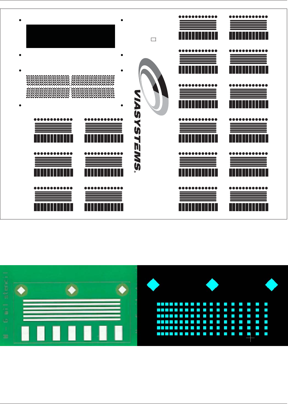
IPC-4556-a6-1
Figure A6-1 Layout of Test Board Used for Solder Spread and Wetting Balance Testing
Solder Spread Test Method The solder spread test pattern consists of 6 parallel traces, each 0.5 mm thick and 25 mm long.
The key aspect of the spread test is the solder paste stencil design shown in Figure A6-2, which consists of 18 solder paste
deposits (0.5 mm x 0.5 mm) on each trace (108 total). The distance between the 18 paste deposits increases linearly across
the pattern, from a minimum of ~ 0.15 mm [6 mils] to a maximum of nearly 1 mm [38 mils].
SOLDERMASK DEFINED
SOLDERMASK CLEARANCE
SS-NN
MERIX
Figure A6-2 Solder Spread Pattern and Paste Stencil – Example of Solder Spread Pattern (left view) and Corresponding Solder Paste
Stencil Openings (right view)
January 2013 IPC-4556
41