IPC-4556 印制板化学镍钯浸金(ENEPIG)规范ENG.pdf - 第53页
IPC-4556-a6-4 Figure A6-4 Solder Spread Results Using an ROL1 Sn/Pb/Ag Solder Paste on ENEPIG Deposits (Note: The ENEPIG deposits are from 7 dif ferent chemistry suppliers (with dif ferent electroless palladium thickness…
During reflow, solder deposits that contact each other tend to coalesce. Across the test pattern, the variation in the gaps
between paste deposits requires the solder to spread more at one end of the pattern for coalescence to occur. The overall
solder spread is calculated by first counting the number of distinct solder deposits remaining in each row of the pattern after
reflow. Then, the counts for the rows (‘‘x’’) are entered into the following equation:
108 −
φ=
Σ
i =l
6
x
i
z
102
100%
The result is a solder spread value expressed as a percent. A pattern exhibiting complete coalescence of the 18 deposits on
each row would achieve a sum of 6 (a count of 1 solder deposit per row x 6 rows), yielding a solder spread of 100%. If none
of the deposits coalesce, the sum is 108 and the solder spread is 0%, as expected. Figure A6-3 shows a solder spread result
of 14%.
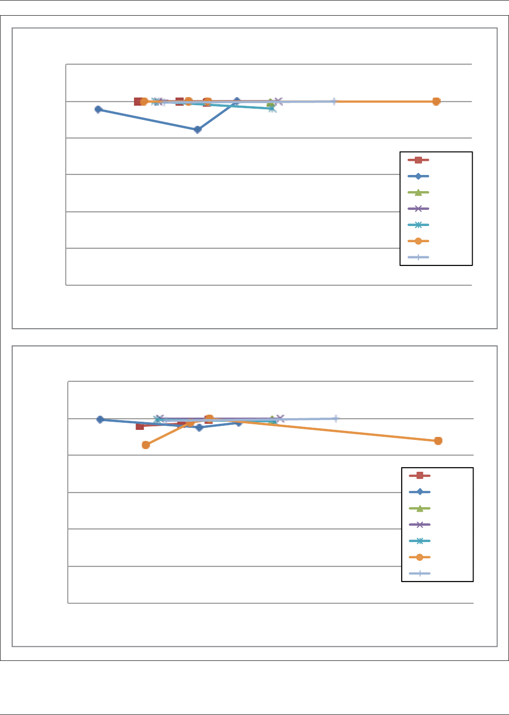
ENEPIG Solder Spread Results:
SnPb Solder
The ROL1 Sn/Pb/Ag solder paste (using a SnPb solder profile) achieved very high solder spread percentages
(>90%) for all samples, regardless of ENEPIG chemistry, electroless palladium thickness, or pre-conditioning. There was no
meaningful differentiation between any of the samples (see Figures A6-4 and A6-5).
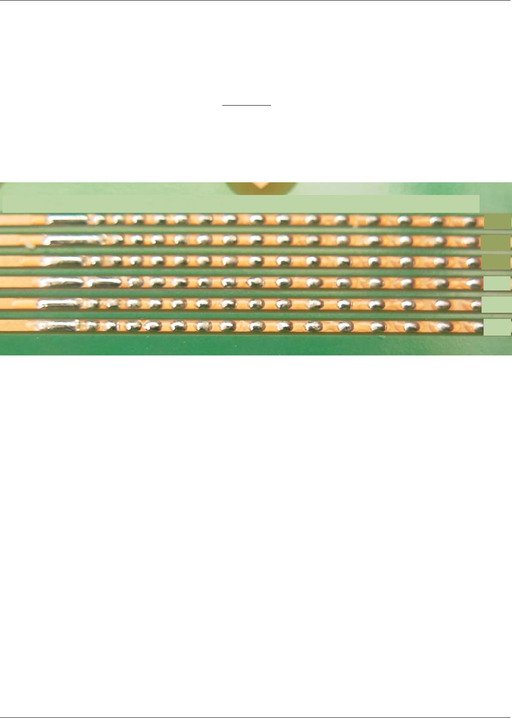
Figure A6-3 An Actual Solder Spread Result Showing the Deposits Counted for Each Line of the Pattern
IPC-4556 January 2013
42
Line 1: 1234567891011121314 15 16
=16
=15
=16
=15
=16
=16
IPC-4556-a6-4
Figure A6-4 Solder Spread Results Using an ROL1 Sn/Pb/Ag Solder Paste on ENEPIG Deposits
(Note: The ENEPIG deposits are from 7 different chemistry suppliers (with different electroless palladium thicknesses) using the solder spread
pattern. The Figure A6-4 - Top is for boards as-received. The Figure A6-4 - Bottom is for soldering after pre-conditioning of the boards for 8
hours at 72 °C [162 °F] and 85% RH).
110%
110%
110%
80%
70%
60%
50%
Solder Spread (%
0.00 0.05 0.10 0.15 0.20 0.25 0.300.35 0.40 0.45 0.50
)
SnPb ROL1 – No Conditionin
Actual Pd Thickness (um)
g
Chem A
Chem B
Chem C
Chem D
Chem E
Chem F
Chem G
110%
110%
110%
80%
70%
60%
50%
Solder Spread (%
0.00 0.05 0.10 0.15 0.20 0.25 0.300.35 0.40 0.45 0.50
)
Actual Pd Thickness (um)
SnPb ROL1 – Post 72 C/85% RH
Chem A
Chem B
Chem C
Chem D
Chem E
Chem F
Chem G
January 2013 IPC-4556
43
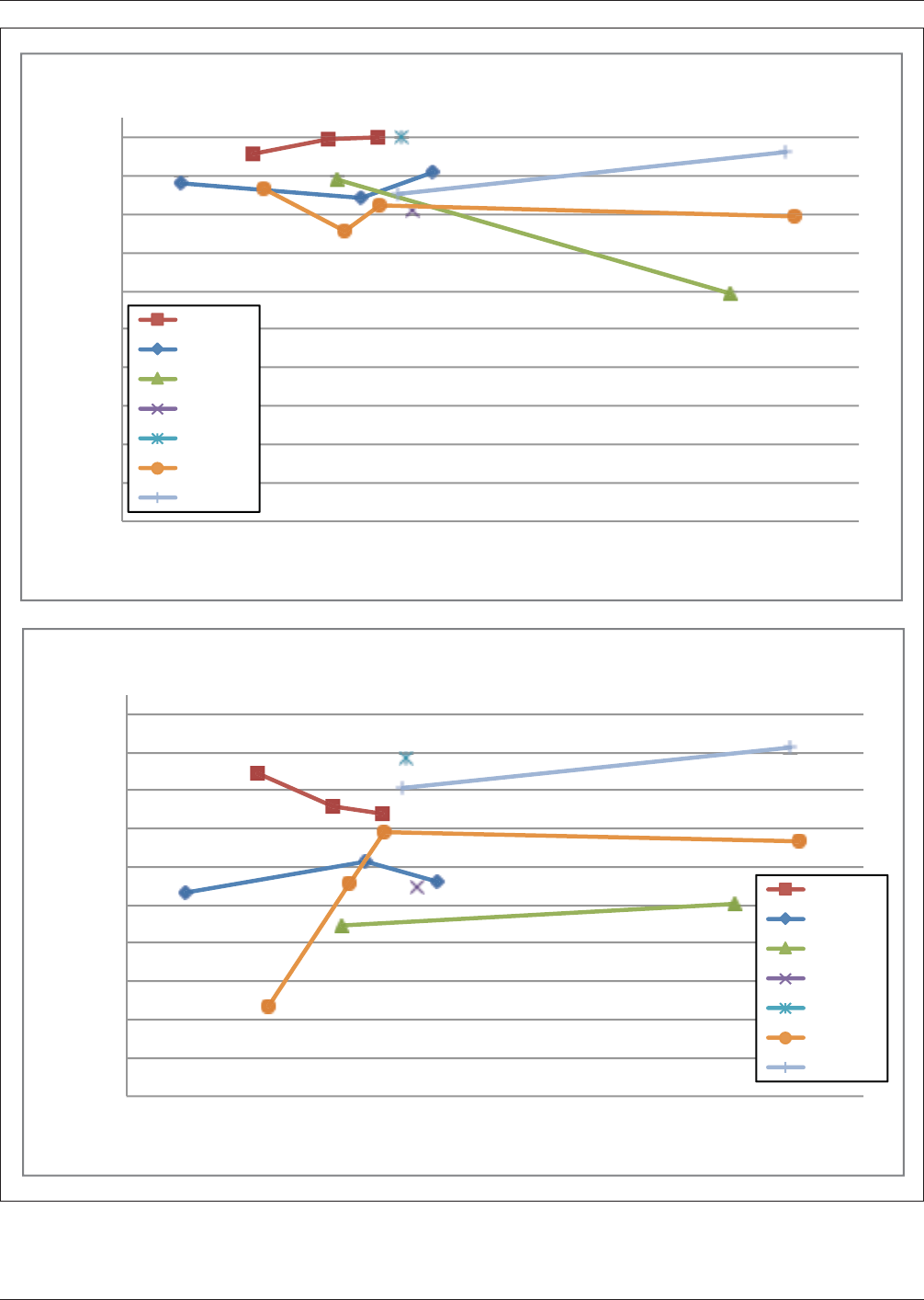
IPC-4556-a6-5
100
Figure A6-5 Solder Spread Results Using an ROL0 Pb-free Solder Paste of the SAC 300 Family on ENEPIG Deposits
(Note: The ENEPIG deposits are from 7 different chemistry suppliers (with different electroless palladium thicknesses) using the solder spread
pattern. The Figure A6-5 - Top is for boards as-received. The Figure A6-5 - Bottom is for soldering after pre-conditioning the boards for 8 hours
at 72 °C [162 °F] and 85% RH).
%
90%
80%
70%
60%
50%
40%
30%
20%
10%
0%
Solder Spread (%
0.00 0.05 0.10 0.15 0.20 0.25 0.300.35 0.40 0.45 0.50
)
Actual Pd Thickness (um)
100%
90%
80%
70%
60%
50%
40%
30%
20%
10%
0%
Solder S
pread (%
0.00 0.05 0.10 0.15 0.20 0.25 0.300.35 0.40 0.45 0.50
)
Actual Pd Thickness (um)
PB-free ROL0 – No Condioning
Chem A
Chem B
Chem C
Chem D
Chem E
Chem F
Chem G
Pb-free ROL0 – Post 72 C/85% RH
Chem A
Chem B
Chem C
Chem D
Chem E
Chem F
Chem G
IPC-4556 January 2013
44