IPC-4556 印制板化学镍钯浸金(ENEPIG)规范ENG.pdf - 第75页
• For samples with thin coatings (<100 nm) and small structures (<0.2 - 0.3 mm) an XRF instrument with a semiconductor detector and special X Ray optics (poly-capillary) is required to achieve suf f icient high int…
APPENDIX 9
XRF Thickness Measurements of thin Au and Pd (ENEPIG):
Recommendations for Instrumentation (Detectors) and their Limitations
Michael Haller
Chief Operating Offıcer
Fischer Technology
• The given limitations in Table A9-1 for the minimal measurable thickness is based on measurements of a typical sample
with 50 nm Au and 100 nm Pd plated on 4 µm Ni, over 30 µm Cu on a substrate of fiberglass-reinforced epoxy resin with
Br for the given total intensities. Measuring time 120 s.
• Intensities are given for reference. If lower intensities are realized for a certain XRF setup appropriate adjustments should
be made, by either increasing collimator size (while still meeting spot size specifications) or by increasing the measure-
ment time.
• Detector limits are derived from repeatability precision (standard deviation) of the XRF instruments and based on count-
ing statistics which directly relate to total intensity and measurement time. As a general rule, in order to improve the repeat-
ability precision by a factor of 2 an increase in intensity or measurement time of a factor of 4 is required.
• The minimum measurable thickness for proportional counter detectors is limited due to the strong influence of the PCB
base material (Br) and Cu thicknesses (background signal and peak overlap).
• The use of calibration standards with similar thicknesses to the specified ENEPIG thicknesses which are to be measured
is recommended. Tri-layer standards where Au and Pd are plated directly on Ni/Cu/PCB should be used for calibration for
Cu thicknesses >30 µm. Tri-layer foil standards where Au and Pd are plated on a Ni-foil should be used if boards with
varying Cu-thickness are to be measured. The foils allow for great flexibility since they can be placed on various base
materials, therefore achieving optimal accuracy. With decreasing Cu thickness the influence of the PCB material becomes
more and more significant and requires careful calibration.
• For Cu thickness >30 µm a combination of a minimum of two calibration standards with approximate thicknesses as below
should be used.
– Au/Pd/Ni/Base 50 nm/20 nm/3 µ
– Au/Pd/Ni/Base 50 nm/90 nm/3 µ
– Au/Pd/Ni/Base 50 nm/300 nm/3 µ
– Au/Pd/Ni/Base 10 nm/20 nm/3 µ
• For Cu thicknesses <30 µm a combination of a minimum of two calibration foil standards with approximate thicknesses
as below should be used
– Au/Pd/Ni 60 nm/20 nm/4 µ
– Au/Pd/Ni 60 nm/60 nm/4 µ
– Au/Pd/Ni 50 nm/100 nm/4 µ
– Au/Pd/Ni 50 nm/250 nm/4 µ
• To verify accuracy, it is most important after the XRF has been calibrated for the appropriate measurement range, that the
instrument will read Au and Pd values of an uncoated board of the measurement sample as statistically zero. Only in this
way can one ensure that no systematic offset in the calibration and setup exists. (i.e., measure on uncoated Ni/Cu/PCB or
Cu/PCB and record Au and Pd values obtained).
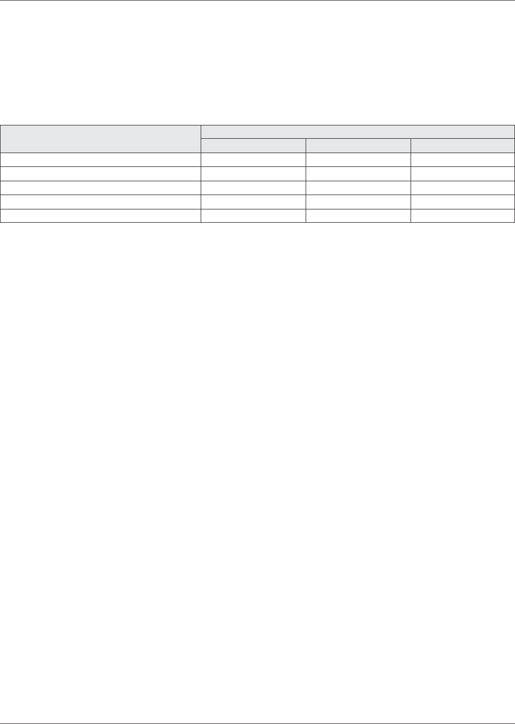
Table A9-1 XRF Detectors and Their Limitations at Typical Count Rates
Detector type
Prop. Counter PIN SDD
Au min ~ 70 - 100 nm ~ 5-10 nm ~ 2 nm
Pd min ~ 100 nm ~ 10 nm ~ 5 nm
Total Intensity 8000 cps 50 000 cps 50 000 cps
PCB and Cu Influence strong medium medium
Typical Energy Resolution for min Kα 900 eV <200 eV <150 eV
IPC-4556 January 2013
64

• For samples with thin coatings (<100 nm) and small structures (<0.2 - 0.3 mm) an XRF instrument with a semiconductor
detector and special X Ray optics (poly-capillary) is required to achieve sufficient high intensities.
• Due to the influence of the base material on the measurements (Br in PCB materials, different composition of the PCB
base materials, varying Cu thicknesses) evaluation software with a peak deconvolution, flexible background correction and
the ability to take the P in the Ni, and Pd layer into account, as well utilizing Pd L and Au M emissions is absolutely nec-
essary for the accuracy of the measurements. The influence is especially large for proportional counter instruments, there-
fore, proportional counter XRF systems are not recommended for Cu thicknesses <30 µm (~ 1 oz).
January 2013 IPC-4556
65

APPENDIX 10
Gage Capability. Gage R&R Type 1 Study
Michael Haller
Chief Operating Offıcer
Fischer Technology
Goal: Test of gage capability with respect to repeatability and mean of measurement values for a given tolerance.
• Preferably the gage capability is conducted with a calibrated reference standard, with its reference value approximately in
the middle of the tolerance field.
• At defined measurement points the reference standard is to be measured with n ≥25 times under repeatability conditions.
• For measurement criteria with Upper and Lower Specification Limits (USL and LSL): T=USL-LSL
• For measurement criteria with only a one-sided specification limit (USL or LSL): T is not existent. In this case the allow-
able measurement value lies below USL -4 s or above LSL +4 s.
• The value of the reference standard should be within ± 10 % of the USL or LSL.
• If Gage capability Indexes are to be calculated. use the following formulas.
(The instrument capability is checked thru the Cg and Cgk values. These are defined as:
Gage capability:
C
g
=
0.2 z T
6 z s
C
gk
=
–
0.1 z T –
|
x–x
m
|
3 z s
–
Where: T = tolerance, s = standard deviation), x
m
= mean of standard and x = mean value measurement.
Note: A gage is considered capable if Cg ≥1.33 and Cgk ≥1.33
IPC-4556 January 2013
66