prober-english.pdf.pdf - 第8页
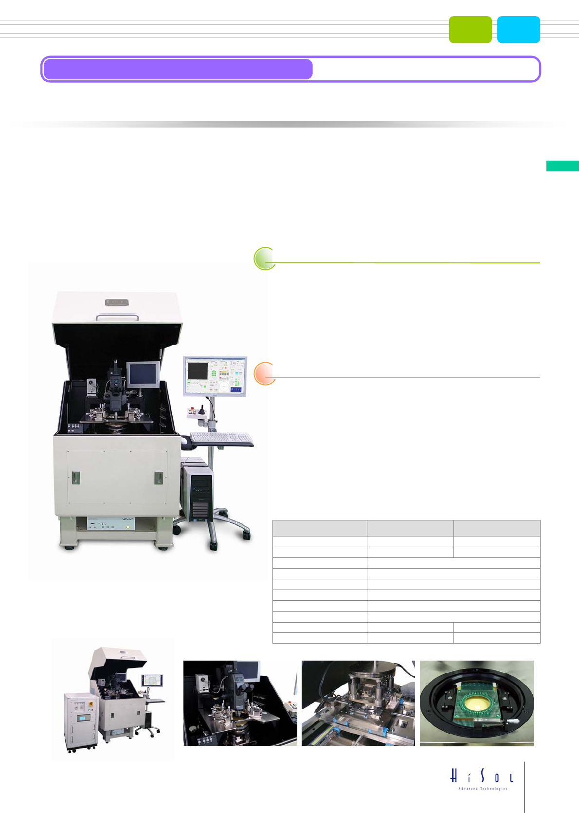
・ Model HSP -200SC is for 8" wafers. ・ Model HSP -300SC is fo r 12" wafers. 8 inch 12 inch ■ SEMI-AUTOMATIC PROBER Semi ‐ Automatic Prober for High /L o w Temperature Tests Applications ‐ Temperature …
■ SEMI-AUTOMATIC PROBER
・
Model HSP-200 is for 8" wafers.
・
Model HSP-300 is for 12" wafers.
8inch 12inch
StandardSemi‐AutomaticProberModel
Thisisastandardsemi‐automaticprobesystemthatsupports8” or12” wafers.
Equippedwithahigh‐accuracyX‐Y‐Z‐θ quadraxial closedloopstagehavingexcellentpositioningaccuracyandrepeatability,
thisprobesystemensuresreliableprobecontact.
Thisprobesystemcanincorporateahotchuckthatsupportsatemperaturerangefrom+20°
Cto+300°C.
Thisprobesystemcanoptionallysupporthigh‐currentandhigh‐voltagepowerdeviceapplications.
Applications
Extended applications
‐ Temperaturecharacteristicstestsinrangefrom+20°Cto+300°C
‐ UltralowsignalI‐Vmeasurements(fAlevel)
‐ VariousC‐Vmeasurements(quasi‐staticC‐V,HF‐CV,andRF‐CV)
‐ RFmeasurements(upto67GHz)
‐ Ultrahigh‐speedI‐Vmeasurements
‐ Probecardsupport(cansupportMultisiteWLR)
‐ Built‐inlasercutter
(Pointmarking,Exfoliationofprotectionlayer,Metallayercutting )
‐ Activevibrationisolatorandultrahigh‐accuracyprobingthrough
imageprocessingpatternrecognition(accuracy:± 1umorfiner)
‐ Light‐receiving/emittingcharacteristicsevaluationapplicationsfor
optoelectronics(suchasLED,LD,VCSEL,
andPD)
‐ Commongatepad contactsofflat‐paneldisplaydevices
‐ High‐powerdevicemeasurements
(200Apulse,±3kVtriaxial,±10kVcoaxial)
‐ Waferlevelreliabilitytests(suchasEM,TDDB,HCI,NBTI,and BT)
WaferSize
X‐Ytravel
X‐Yrepeatability
X‐Yaccuracy
Ztravel
Unitdimension(W×D×H)*
Weight*
Zrepeatability
HSP‐200 HSP‐300
~φ200mm ~φ300mm
X:205mm,Y:300mm X:310mm,Y:450mm
1300×1000×1550mm
1400×1050×1600mm
750kg 950kg
<±2μm
<±5μm
20mm
<±1μm
θ travel
θ repeatability
±7.5°
0.002°
*Itemswithasteriskvarydependingonsystemconfiguration.
Model HSP-200 / HSP-300
7
Semi‐AutomaticProber
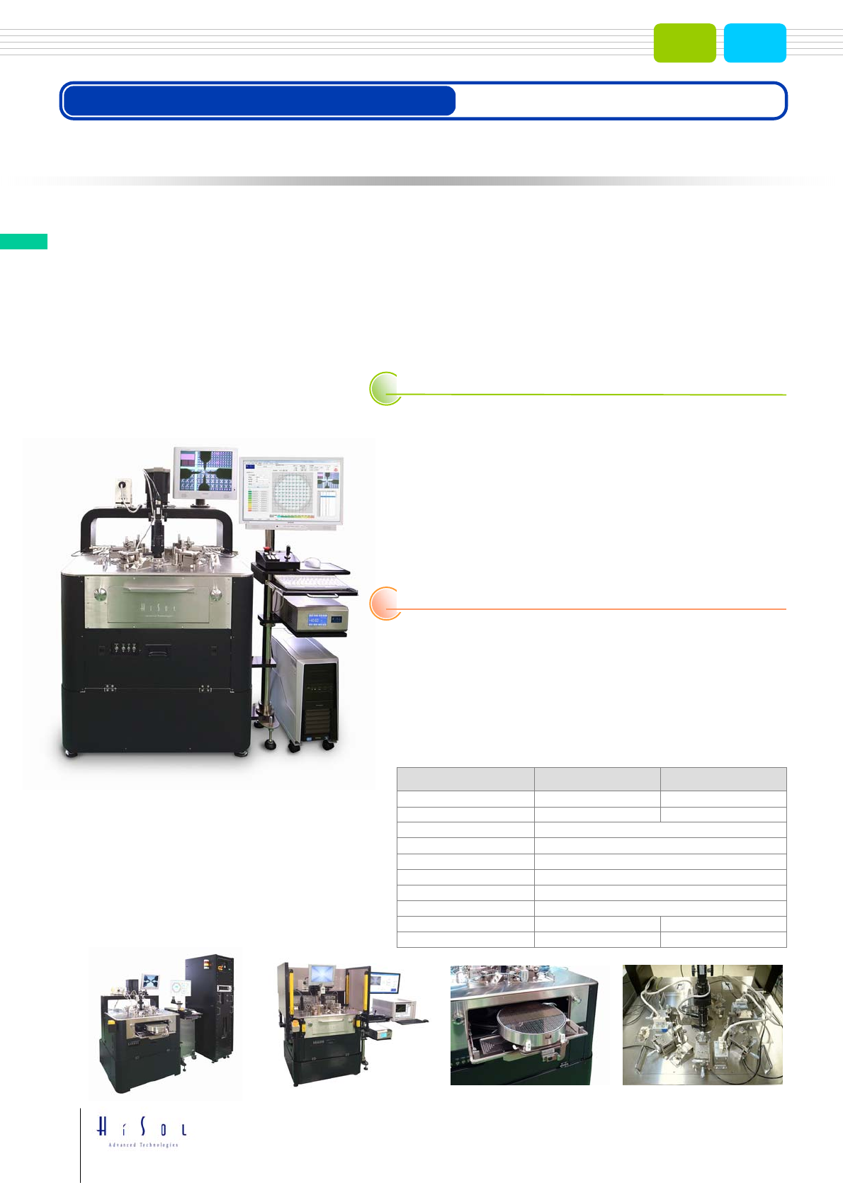
・
Model HSP-200SC is for 8" wafers.
・
Model HSP-300SC is for 12" wafers.
8inch 12inch
■ SEMI-AUTOMATIC PROBER
Semi‐Automatic ProberforHigh/LowTemperatureTests
Applications
‐ Temperaturecharacteristicstestsinrangefrom+25°Cto+300°C
orfrom‐60°Cto+300°C
‐ UltralowsignalI‐Vmeasurements(fAlevel)
‐ VariousC‐Vmeasurements
(quasi‐staticC‐V,HF‐CV,andRF‐CV)[subpFlevel]
‐ 1/fnoiseevaluation
‐ RTN(random telegraphnoise)evaluation
‐ High‐frequencynoiseevaluation(upto800MHz)
‐ RFmeasurements(upto67GHz)/Sparameteracquisition
‐ Ultrahigh‐speedI‐Vmeasurements
Thisisasemi‐automaticprobesystemfornext‐generationsemiconductordevicesdesignedforlownoiseandlowleakage.
Inthissystem,ashieldedchamberstructurecontains
theprobeandchuckinatotallyEMIshieldedenvironment.
Thesystemsupportsin‐planeautomaticmeasurementssuchasultralowsignalI‐V/C‐Vmeasurementinthreshold
regions,1/fnoisemeasurement,Sparameteracquisition,RTN(randomtelegraphnoise)measurement,andhigh‐speedI‐V
measurementinatemperature
controlrangefrom‐65°Cto+300°C(or+400°Cwhenusingthespecialoption).
Thisprobesystemcanoptionallysupporthigh‐currentandhigh‐voltagepowerdeviceapplications.
*TheHSP‐150SCfor6” wafersisalsoavailable.
Extended applications
‐ Probecardsupport(cansupportMultisiteWLR)
‐ Activevibrationisolatorandultrahigh‐accuracyprobingthrough
image processingpatternrecognition(accuracy:±1umorfiner)
‐ Light‐receiving/emittingcharacteristicsevaluationapplicationsfor
optoelectronics(suchasLED,LD,VCSEL,andPD)
‐ Commongatepad contactsofflat‐paneldisplaydevices
‐ High‐powerdevicemeasurements
(400Apulse,±3kVtriaxial,±10kVcoaxial) *8” model
‐ Waferlevelreliabilitytests(suchasEM,TDDB,HCI,NBTI,and BT)
WaferSize
X‐Ytravel
X‐Yrepeatability
X‐Yaccuracy
Ztravel
Unitdimension(W×D×H)*
Weight*
Zrepeatability
HSP‐200SC HSP‐300SC
~φ200mm ~φ300 mm
X:205mm,Y:205mm X:310mm,Y:310mm
1350×1000×1450mm
1450×1150×1450mm
1050kg 1250kg
<±3μm
<±5μm
20mm
<±1μm
θ travel
θ repeatability
±7.5°
0.002°
*Itemswithasteriskvarydependingonsystemconfiguration.
Model HSP-200SC / HSP-300SC
Semi‐AutomaticProber
8
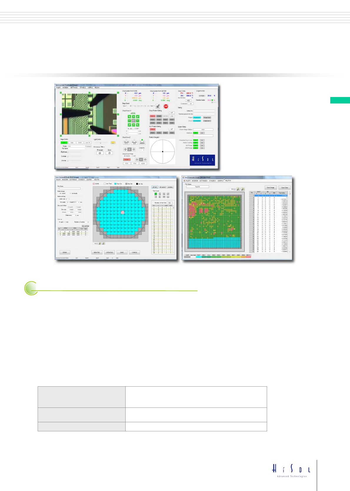
HiSOLSemi‐Automatic Prober ControlSoftware
Manualoperation
BINmapping
WaferMapsetting
Seals feature
Supportedautomaticmeasurementsoftware
KEYSIGHTtechnologies
‐EasyEXPERT
‐DesktopEasyEXPERT
‐WaferProExpress
TFF/KEITHLEYinstruments
‐4200‐SCS KITE(KeithleyInteractiveTestEnvironment)
‐ACS
Proplus designsolution ‐Noisepro
OtherGP‐IBcommunication‐enabledsoftware
‐ User‐friendlymultifunctionalsemi‐automaticprobingsoftware.
‐ SupportsWindows8asitsoperatingsystem.(Windows7isalsosupported.)
‐ AlsoavailableasamanualproberwithasoftwareGUIorjoystickcontroller.
‐ ReceivingBINinformationfromahigher‐levelmeasuringinstrument,itispossibletodisplayBINmapping.
‐ Supportswafer
thermalexpansioncompensationfunctionforThermaltest.
‐ Possibletocontrolthesemi‐automaticproberusingtheGP‐IBcommandsentfromahigher‐levelmeasuring
instrument or PC.
‐ Possibletoprovidesoftwareformakingadatabaseofandextractingparametersofrawdataobtainedfromeach
measuring instrumentinordertoanalyzethedata.
(Optional)
‐ Theself‐developedsoftwareallowsuserstoincorporatecustomizedrequirements.
■ SEMI-AUTOMATIC PROBER
Semi‐AutomaticProber
9