N7201A652E.pdf - 第488页
NPM- TT2 EJM1E E-MB-06O-04 Specifi- cation A pplica ble PCB specifica tions 1 6-1-4 -1 Operating procedure 6-1-4 Item Specification PCB dimensions PC size 300mm transfer specificatio ns Dual lane mode ● Min: L 50 × W 50m…
NPM-TT2 EJM1EE-MB-06O-04
At
a glance
6-1-3-4
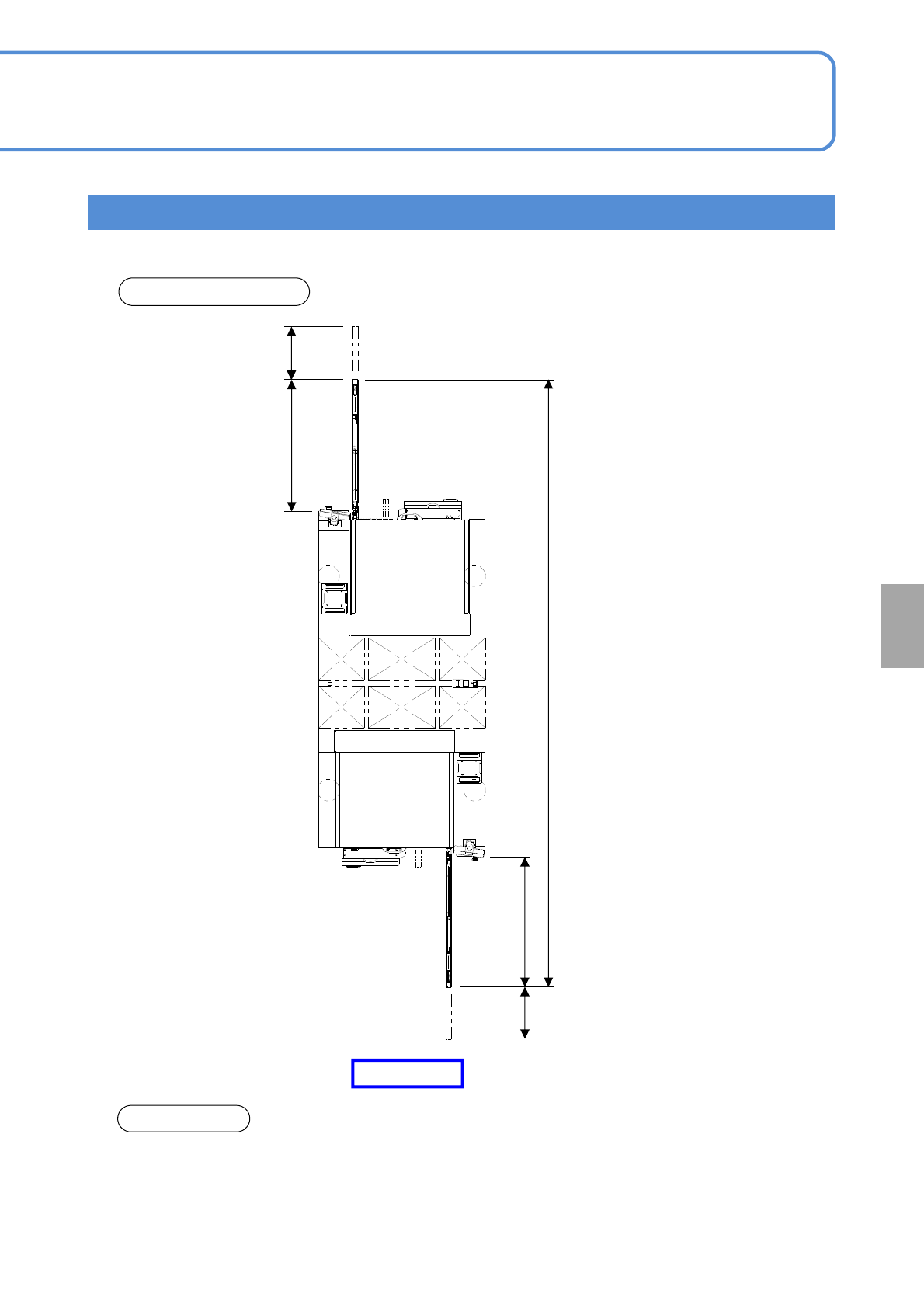
When the stackable stick feeder is installed
(Unit: mm)
Outside dimensions
Front side
4 619
400 996
400996
NOTE
To remove/insert stackable stick feeders, the following working areas are required:
● 400 mm behind the stick feeder, as shown above, when removing/inserting feeders
in order from the end
● Max. 1 600 mm if the one in the middle of three adjoining stick feeders is removed/inserted
(Required for moving along the entire length of the feeder)
NPM-TT2 EJM1EE-MB-06O-04
Specifi-
cation
Applicable PCB
specifications 1
6-1-4-1
Operating procedure
6-1-4
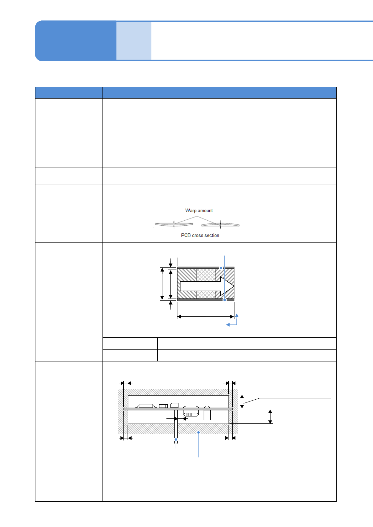
Item Specification
PCB dimensions
PC size
300mm
transfer specifications
Dual lane mode
●Min: L 50 × W 50mm ●Max: L 510 × W 300mm
Single lane mode
●Min: L 50 × W 50mm ●Max: L 510 × W 590mm
PCB dimensions
M size 260mm
transfer specifications
Dual lane mode
●Min: L 50 × W 50mm ●Max: L 510 × W 260mm
Single lane mode
●Min: L 50 × W 50mm ●Max: L 510 × W 510mm
Thickness
(mm)
0.3 to 8.0
Mass (kg)
1.5kg or under (after placement)
Allowable PCB warp
(mm)
Placement area
(mm)
Dual lane mode a:50 to 300 b:44 to 294 c:3.0 d:50 to 510
Single lane mode a:50 to 590 b:44 to 584 c:3.0 d:50 to 510
Dead space
(mm)
3
28
No component area
PCB support pin
Keep 2 mm away from the component on the reverse side.
●If you want to create your own PCB-support blocks, please consult us.
Warp lower: within 0.5
Warp upper: within :0.5
3
3
3
*1)
Y
X Fixed side
a b
c
d
c
PCB flow
No component area
*1)
8-nozzle head : Max. 12
3-nozzle head : Max. 28
NPM-TT2 EJM1EE-MB-06O-04
6-1-4-2
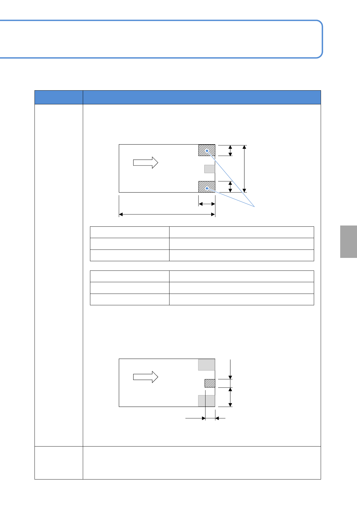
Item Specification
PCB cutout
condition
PCB cutout size should meet the following two conditions.
■Condition A
PCB cutout size should meet the following condition.
■Condition B
There should be no cutout (including slit) in the area B shown below.
PCB
projection size
from PCB
edge
Consult us.
L
L1
50 mm ≦ L ≦ 350 mm
L/4 or less
350 mm < L ≦ 510 mm
Smaller one of either L/4 or 100 mm
●Above described condition is when the PCB thickness is less than1.6 mm. If the
PCB thickness exceeds 1.6 mm, please consult us.
W
W1
50 mm ≦ L ≦ 300 mm
Smaller one of either W/3 or 30 mm
300 mm < L ≦ 590 mm
Consult us separately
Transport
direction
L
L1
A
A
W1
W1
W
Any of one location
30mm
Transport
direction
10mm
B
10mm
●If there is cutout (including slit) in the above area, please consult us.
At
a glance