N7201A652E.pdf - 第490页
NPM- TT2 EJM1E E-MB-06O-04 Specifi- cation A pplica ble PCB specifica tions 2 6-1-4 -3 Operating procedure 6-1-4 Item Specification PCB recognition mark ■ Examples of ma rk shap e ● PCB rec ognition implements comp ensat…
NPM-TT2 EJM1EE-MB-06O-04
6-1-4-2
Item Specification
PCB cutout
condition
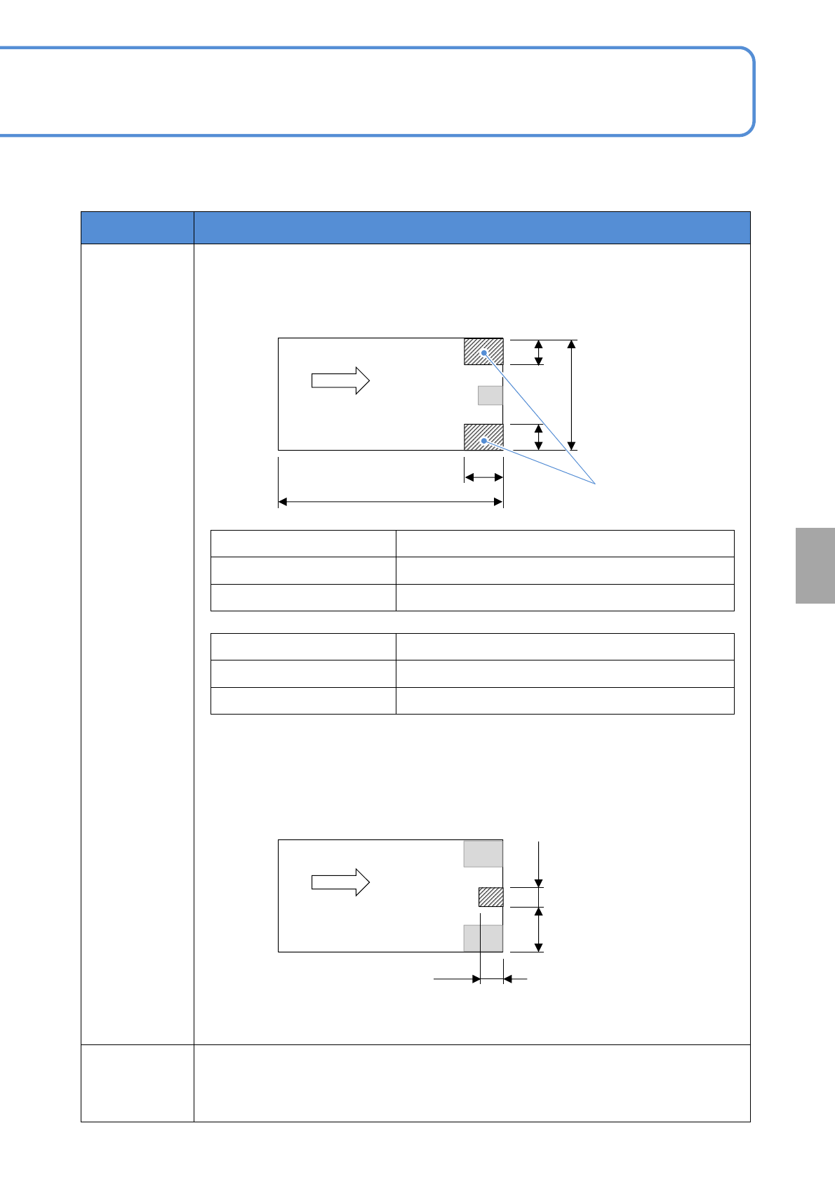
PCB cutout size should meet the following two conditions.
■Condition A
PCB cutout size should meet the following condition.
■Condition B
There should be no cutout (including slit) in the area B shown below.
PCB
projection size
from PCB
edge
Consult us.
L
L1
50 mm ≦ L ≦ 350 mm
L/4 or less
350 mm < L ≦ 510 mm
Smaller one of either L/4 or 100 mm
●Above described condition is when the PCB thickness is less than1.6 mm. If the
PCB thickness exceeds 1.6 mm, please consult us.
W
W1
50 mm ≦ L ≦ 300 mm
Smaller one of either W/3 or 30 mm
300 mm < L ≦ 590 mm
Consult us separately
Transport
direction
L
L1
A
A
W1
W1
W
Any of one location
30mm
Transport
direction
10mm
B
10mm
●If there is cutout (including slit) in the above area, please consult us.
At
a glance
NPM-TT2 EJM1EE-MB-06O-04
Specifi-
cation
Applicable PCB
specifications 2
6-1-4-3
Operating procedure
6-1-4
Item Specification
PCB
recognition
mark
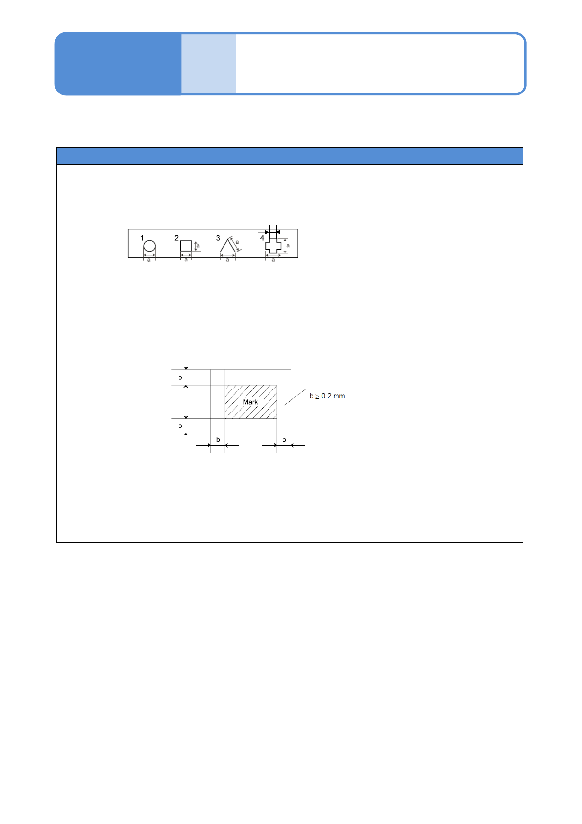
■Examples of mark shape
●PCB recognition implements compensation through the use of the physical relationship
between recognition marks and a circuit pattern.
●A fixed contrast is required between recognition marks and a PCB.
■Recognition mark dimensions and background
●The background of a mark requires the noninterference area - larger than certain
dimensions- outside the mark itself.
●Marks are not always black in color.
■Recognition mark position
●Two PCB recognition marks are required on opposing corners of a PCB.
Triangle on the 3rd figure on the left:
Equilateral triangle
Line width on 4th figure on the left:
0.3 mm or more
0.5 mm ≦ a ≦ 1.6 mm
0.3 mm ≦ c
c
Noninterference area
NPM-TT2 EJM1EE-MB-06O-04
At
a glance
Specifi-
cation
6-1-5-1
Item Specification
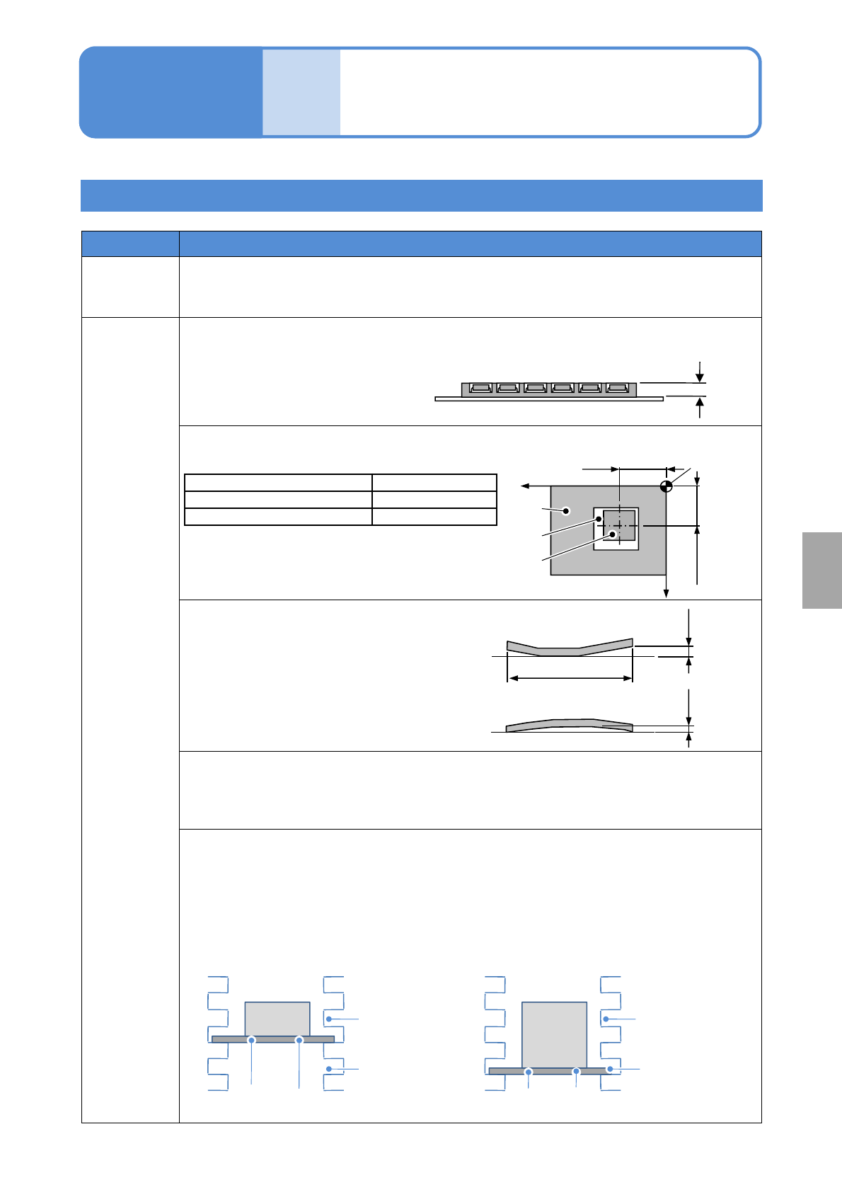
Component
Dimensions: Max 150 25 mm (Diagonal side 152.1 mm)
Thickness: Max 30 mm
Mass: Max. 30 g
Tray
■Tray outside dimensions
●Max.
L 230 W 335 H33mm
●Min.
L 85 W 100 H2mm
■Relationship between component pickup surface and position error
●The component pickup surface
should be flat.
■Warp (Clearance)
■Type
●For enough strength and dimensional accuracy, a tray should be injection-molded.
●Other than the above, we check your sample trays and suggest optional trays or
customization on costs.
■Loading the tray feeder pallet (option), the tray feeder magazine (option)
Condition
●Weight of a tray (including components) on a tray feeder pallet : 1 kg or less.
●Weight of a tray feeder magazine (including a tray feeder pallet, a tray, components) : 20
kg or less per magazine.
●Limitation of a tray feeder pallet insertion
・11 mm < tray height ≦ 26 mm ・26 mm ≦ tray height ≦ 33 mm
2to33mm
Component pickup surface Position error
10 10 mm or less 1.0 mm or less
10 10 mm or over 1.5 mm or less
Maximum 0.5 mm
Component tray
Tray
Not Insertable
at the top
Pallet
Magazine
Tray
Not insertable
at the top and
second level
Pallet
Magazine
Tray
Tray
Max. 335 mm
Operating procedure
6-1-5
Clearance
Clearance
Xw + Position error
Yw+Position
error
Tray setting
reference point
(Tray origin)
Tay
Component
X
Y
Pocket
Component/tray
specifications Intelligent
feeder specifications 1