OM-1683-001_w.pdf - 第30页
13 OM-1683 7. "PCB XFER" Window This window enables the operator to move the PCB on each block on each lane on the conveyor to the next block. Reference Refer to "6. "PCB XFER" W indow" in C…
12
OM-1683
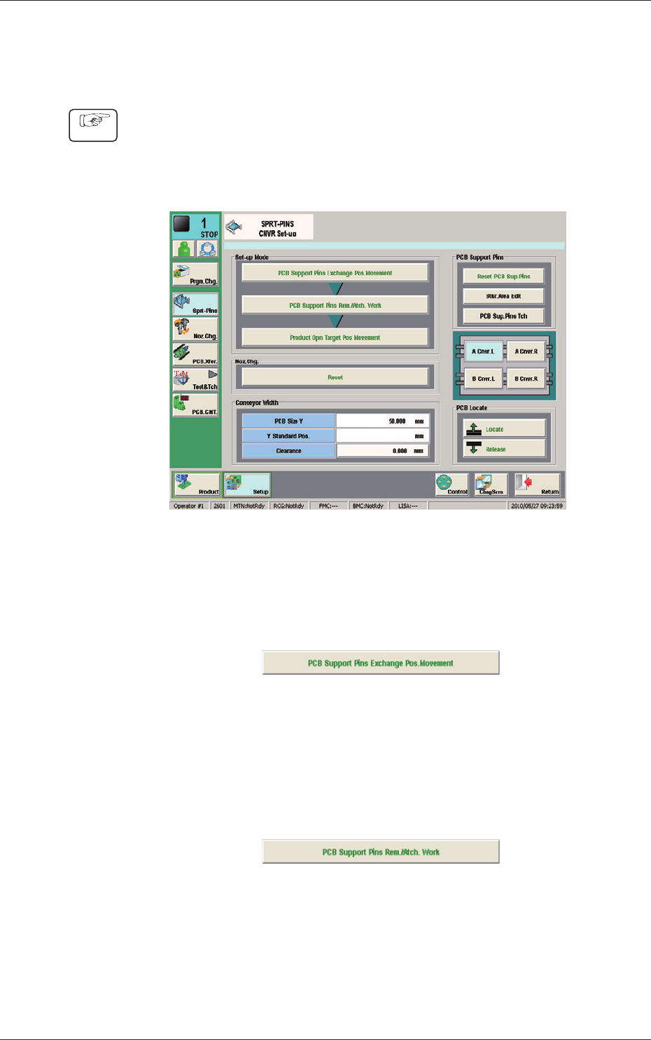
6.1 Collection of PCB Support Pins and Setup Operation of
Conveyor Width
(1) Display the "SPRT-PINS CNVR Set-up" window using the following icon
procedure.
(2) Select the conveyor in the lane where the operation is
performed.
--
Fig. 11
(3) Press the [PCB Support Pins Exchange Pos. Movement] button.
After that, press the [START] button on the operation panel in 10 sec.
(The machine retracts the head and maximizes the conveyor width.)
Fig. 12
(4) Press the [PCB Support Pins Rem./Atch. Work] button and within 10
seconds, press the [START] button on the operation panel.
(The PCB support pins are arranged onto the positions specied in the
pattern program).
Fig. 13
(5) Press the [Product Opn Target Pos.Movement] switch and within 10 seconds,
press the [START] button on the operation panel.
The support pins are moved based on the pattern program where the
conveyor width has been selected.
Procedure
1103-001
6.1 Collection of PCB Support Pins and Setup Operation of Conveyor Width
13
OM-1683
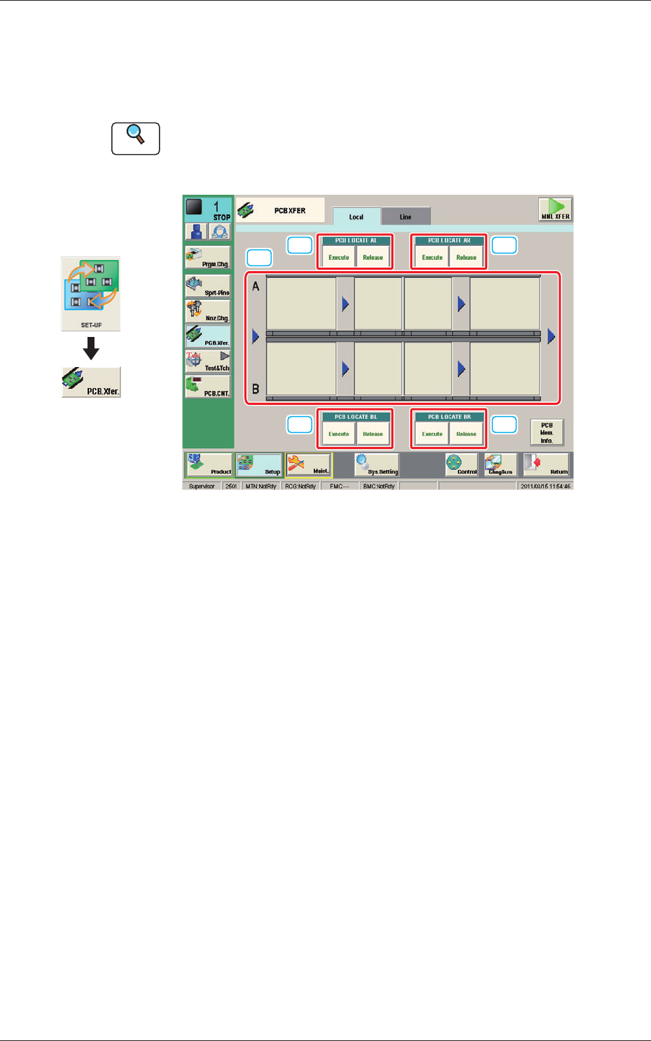
7. "PCB XFER" Window
This window enables the operator to move the PCB on each block on each
lane on the conveyor to the next block.
Reference
Refer to "6. "PCB XFER" Window" in Chapter 6, Volume 2, in the
SIGMA-G5 main machine instruction manual for the information other
than for dual transfer.
[1]
[2] [2]
[2] [2]
Fig. 14 PCB XFER
[1] Conveyor Image Display Pane
Each block in the graphic image of the conveyor is provided with a button
function.
When the [START] button on the operation panel is pressed in 10 seconds
after a conveyor block button, the PCB is transferred to the block position.
[2] PCB LOCA
TE (PCB LOCATE AL, AR, BL, BR)
Using these buttons, the PCB positioning is performed for each lane and
each block.
When the [START] button on the operation panel is pressed in 10 seconds
after the [Execute] button, the backup base of the selected stage moves up
and the PCB is positioned.
When the [START] button on the operation panel is pressed in 10 seconds
after the [Release] button, the backup base moves down and the PCB
positioning is released.
Graphic
Development
1103-001
7. "PCB XFER" Window
14
OM-1683
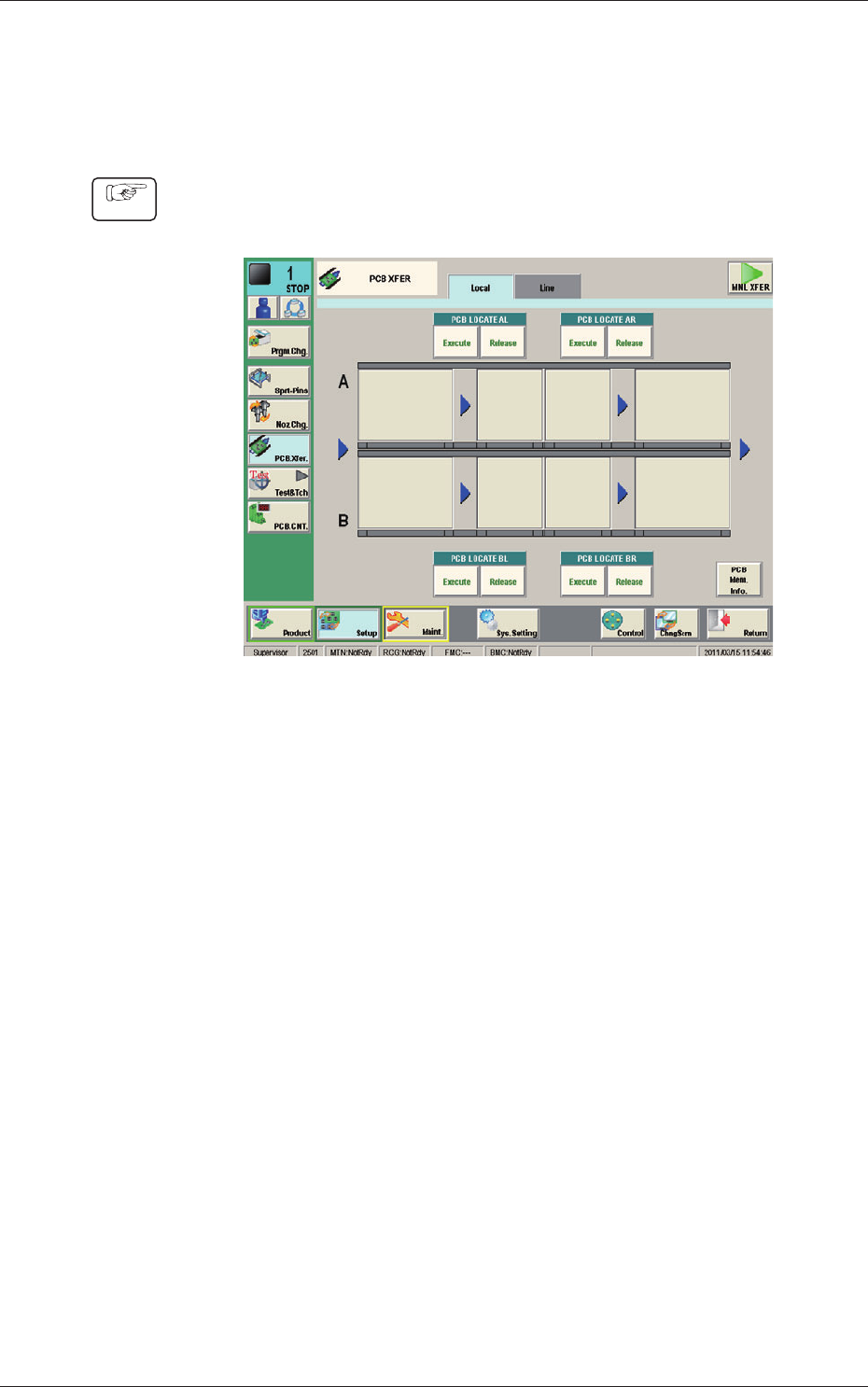
7.1 ConrmationofPCBTransferandPositioning
The following describes how to check the status of the PCB transfer and
positioning in the "PCB XFER" window (a menu of "AUTO OPN").
Procedure
(1) Display the "PCB XFER" window using the following icon procedure.
Fig. 15
(2) Send the PCB in the lane where the PCB transfer and positioning status are
conrmed with the input machine.
(3)
Select a desired block button (expressed graphically) for "PCB LOCATE 1".
In 10 seconds, press the [START] button on the operation panel to transfer
the PCB.
(4)
Conrm that the PCB can be transferred normally and move smoothly
without falling down during the transfer.
(5)
Press the [Execute] button (entitled "PCB LOCATE L").
In 10 seconds, press the [START] button on the operation panel.
(The backup base moves up. )
(6)
Press the cover lock switch to turn off the lamp.
(The transparent cover is unlocked. )
1103-001
7.1ConrmationofPCBTransferandPositioning