ASMPT_Brochure_SIPLACE_CA2_EN_241023 - 第4页
( Edition 4/10-2024 | All rights reserved. | Order No.: A22-ASMPT-A330-EN | Printed in Germany | © ASMPT GmbH & Co. KG All information and illustrations in this brochure are provided “as is” and without any warrantie…
THE HYBRID SIPLACE CA2 HIGH-SPEED PLATFORM
REVOLUTIONIZES SiP PRODUCTION
Only consistent miniaturization and increasingly complex electronics
make things like smart devices, autonomous driving and the 5G commu-
nication standard possible. The key technology is system-in-package
(SiP) because it combines ICs and SMT components into a compact,
highly innovative system.
As a hybrid combination of a SMT placement machine and a die bonder,
the new SIPLACE CA2 can process SMDs supplied from changeover tables
and feeders as well as dies taken directly from a sawn wafer in a single
workstep. By integrating the complex die bonding process into the SMT
line it eliminates the need for special machines in production. Reduced
personnel deployment, high connectivity and integrative data utilization
make the new SIPLACE CA2 the perfect match for the Intelligent Factory.
Placement directly from the wafer: more cost-eective and sustainable
Direct placement from the wafer eliminates the entire die taping process.
The result: less replenishment or splicing, less eort to feed material
to the line. Eliminating the tape feed for the sensitive dies also reduces
handling risk and increases production resiliency. All of these factors add
up to a signicant reduction in costs. At the same time, taping waste is
eliminated, making the manufacturing more environmentally friendly
and sustainable overall, while increasing ROI.
SMT AND DIE BONDING:
SIPLACE CA2
Placement Head CP20
▪ Component spectrum: 0201metric to
8.2 mm × 8.2 mm × 4 mm
▪ Touchless pickup and placement
▪ Placement force: 0.5 N – 4.5 N
▪ Extremely fast: Up to 38,000 cph
▪ Extremely precise: Up to ±10 µm @ 3 σ
Flexible combination
SMT and die bonding in one line simplify your
process ow and improve material logistics.
Space for JEDEC
tray feeder in case
Wafer Exchange
Unit is not used
5 × 8-millimeter
tape-and-reel
feeder
Place for
Multi Wafer
System
2.56 m
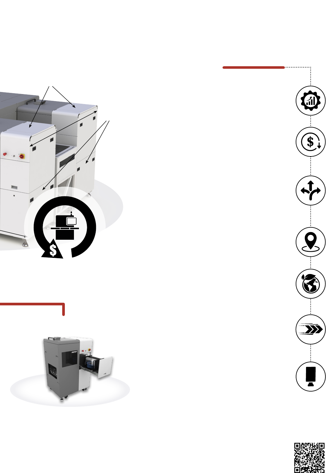
The SIPLACE CA2 can amortize itself
within a year by saving 800 km of tape
per year with full SiP production in
24/7 operation.
Maximum productivity
Processes SMT components and dies directly
from the wafer with die-attach and ip-chip
processes in the same work step.
Cost-saving
No taping cost, no associated quality cost of the die
taping process and no eorts for tape-waste disposal.
Unique exibility
Wafer system for up to 50 dierent wafers with a
wafer swap time of less than 10 seconds (“full multi-die
capability”). A wafer chuck, ux (linear) dipping unit (LDU)
and 10 x 8 mm tape-and-reel feeder tracks can be used
parallel to pick up from wafer.
Full traceability
Keep track of data for each die from its source
on the wafer to its placement position on the
circuit board (“full single-die-level traceability”).
Consistent sustainability
Processing dies directly from the diced wafer eliminates
the entire die-taping process – and lots of tape waste.
Maximum performance
Thanks to die buering and process parallelization,
the SIPLACE CA2 can place up to 54,000 components
per hour directly from wafer with an accuracy
of up to 10 μm @ 3 σ.
Comprehensive quality management
Multiple high-end vision system reliably
recognize even the smallest components and
elements for comprehensive process control.
MULTITALENT COMBINES
TWO WORLDS IN ONE MACHINE
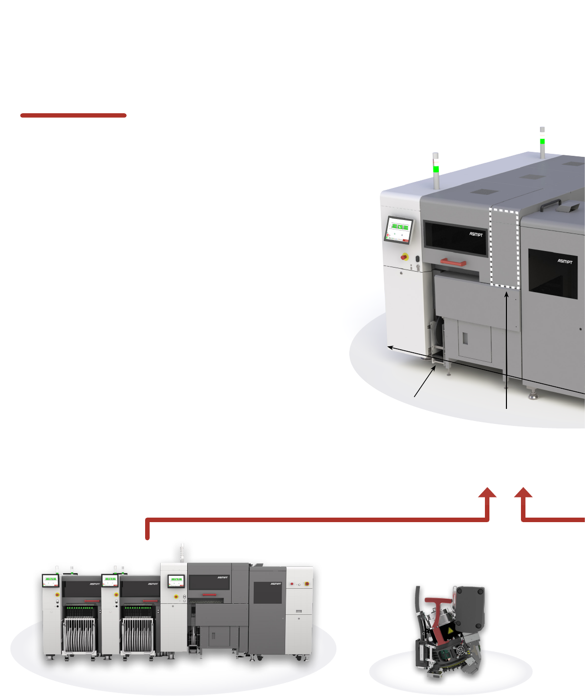
Wafer Exchange Unit
▪ Extremely exible: Processes
up to 50 dierent wafers
▪ Extremely fast: Wafer swap in
only 10 seconds
More about
SIPLACE CA2
Access for
Overhead Hoist
Transport
Wafer Exchange Unit
with wafer swap in
10 seconds
Drawer for
wafer
magazine
2.5 m
2.56 m
1
Y
E
A
R
(
Edition 4/10-2024 | All rights reserved. | Order No.: A22-ASMPT-A330-EN | Printed in Germany | © ASMPT GmbH & Co. KG
All information and illustrations in this brochure are provided “as is” and without any warranties of any kind, whether expressed or implied, including but not limited to,
implied warranties of satisfactory quality, tness for a particular purpose and/or correctness.
The contents of this brochure are for general information purposes only, do not constitute advice, and are subject to change without notice. ASMPT therefore makes no
warranties or representations regarding the use of the content, details, specications or information contained in this brochure in terms of their correctness, accuracy,
adequacy, usefulness, timeliness, reliability or otherwise, in each case to the fullest extent permitted by law. Please contact ASMPT for the most current information.
Any specic performance features and/or capabilities will only be binding if contractually agreed upon.
All product names are brands or trademarks of ASMPT or other suppliers. Unauthorised use by third parties may violate the rights of their owners.
ASMPT GmbH & Co. KG
Rupert-Mayer-Strasse 48 | 81379 Munich | Germany | Phone: +49 89 20800-22000 | Email: smt-solutions.de@asmpt.com
asmpt.com | smt.asmpt.com
SIPLACE CA2
SIPLACE CA2
Placement speed (benchmark)
SMT up to 76,000 cph
Flip chip from wafer
up to 51,000 cph
Die attach from wafer
up to 54,000 cph
Wafer swap 10 seconds
Placement accuracy (3 σ) 20 μm / 15 µm / 10 μm (can be selected on placement position and component shape level)
20 µm @ 3 σ 15 µm & 10 µm @ 3 σ
PCB dimensions
(l × w)
50 mm × 45 mm to 375 mm × 260 mm (dual-lane mode)
50 mm × 45 mm to 375 mm × 430 mm (single-lane mode)
50 mm × 55 mm to 250 mm × 100 mm
Machine dimensions
(l × w × h) 2.56 m × 2.50 m × 1.85 m
Feeder slots
up to 80 × 8-millimeter tape-and-reel feeder or up to
2 × Multi Wafer System and 10 × 8-millimeter tape-and-reel feeder
Power consumption
(average) 1.9 kW
Air consumption 120 Nl/min (2 x SIPLACE CP20)
Certifications CE, SEMI S2/S8, Clean room class ISO 7
Data interfaces IPC-HERMES-9852, IPC-CFX, IPC-SMEMA-9851, SECS/GEM
Placement head SIPLACE CP20
Component range
from tape-and-reel: 0201m up to 8.2 mm
× 8.2 mm
from wafer: 0.3 mm
× 0.3 mm up to 8.2 mm × 8.2 mm
Min. lead pitch 70/50* µm
Min. lead width 30/25* µm
Min. ball pitch 100/50* µm
Min. ball diameter
50/25* µm
* with optional high-resolution camera (SST49)