ASM-SX-V3-设备性能参数-DMS - 第35页
35 Component feeding SIPLACE JTF-M Technical data SIPLACE JTF-M Width 177 mm Height 587 mm JEDEC waffle pack tray specifica- tion Storage capa city W affle pack tray , thin 18 JEDEC w affle pack trays Thick waffle p ack …
34
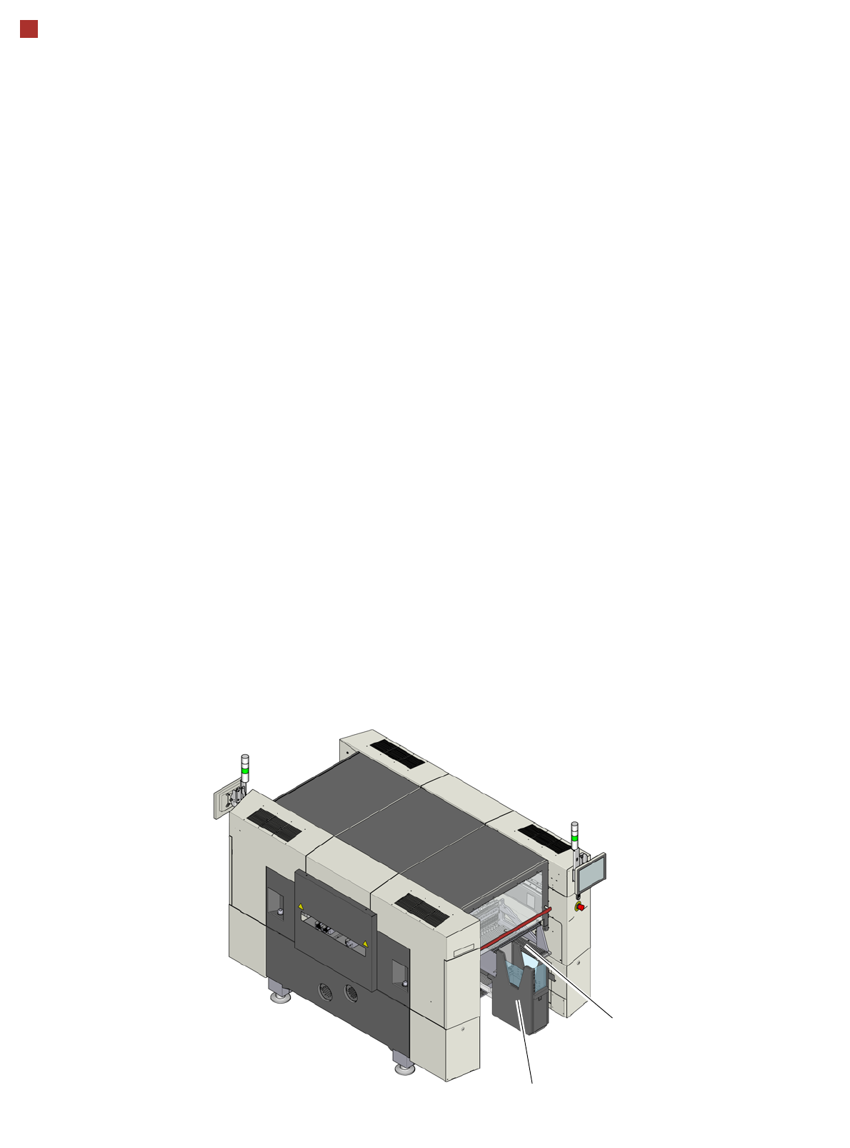
Component feeding
SIPLACE JTF-M
The SIPLACE JTF-M is an
automatic and fast changer
for standard JEDEC waffle
pack trays. On SIPLACE
SX1/SX2 machines, a JTF-M
tray feeder can be installed
on a fixed table instead of a
component trolley. The
SIPLACE JTF-M occupies a
fixed area of tracks on the
fixed table.
Depending on the magazine
type, the SIPLACE JTF-M
stores up to 18 thin or 14
thick JEDEC waffle pack
trays in an exchangeable
cassette and supplies them
as required. The placement
machine can therefore be
supplied with different com-
ponent types at variable
changeover times.
JTF-M
Fixed component table

35
Component feeding
SIPLACE JTF-M
Technical data
SIPLACE JTF-M
Width
177 mm
Height
587 mm
JEDEC waffle pack tray specifica-
tion
Storage capacity
Waffle pack tray, thin 18 JEDEC waffle pack trays
Thick waffle pack tray 14 JEDEC waffle pack trays
Waffle pack tray changeover time
Slot n to n+1 3.5 seconds
Slot 1 to 18 10 seconds
Slot 18 to 1 8.9 seconds
Cassette
Dimensions approx. 330 mm x 150 mm x 230 mm
Max. load capacity 2.7 kg (150 g each for 18 slots)
Pneumatics
5.2 bar to 9 bar
Compressed air consumption
< 28.3 NL/min.
36
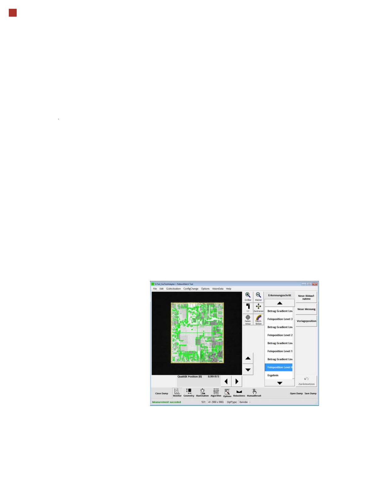
SIPLACE Vision
OnBoard Inspection and Pattern Matching
OnBoard Inspection
The OnBoard PCB Inspec-
tion (SW option) uses the
PCB camera to inspect criti-
cal areas of the board, spec-
ified by the user, e.g. under
BGA or shields just before or
after placement, to make
sure that all components
were placed or to make sure
that there are no objects in
the way of the placement
process.
It is also possible to inspect
the solder paste to make
sure that it is present. How-
ever, this must always be
performed at the first place-
ment machine, before any
placement begins.
A requirement for all inspec-
tion tasks is that a "good pat-
tern" has been saved before
starting.
Pattern Matching
Pattern matching can be
used for components with
very fine contact pads, which
can not be detected with the
existing component camera
resolution. Searching and
detection is performed over a
larger area, which contains
unique structures (patterns).
Once the specified area has
been detected, the compo-
nent is aligned and placed
according to the position of
this area and in relation to the
substrate.