XCEED-BSI-TIIHTRONICS.pdf - 第2页
P ARMI MEXICO W T CG T orres Corporativas Av . Rinconada de las Praderas #1249 B-303 Col. V alle Verde C.P . 44550 Guadalajara, Jal. México +52 81 1015 7866 www.parmi.com info@tiihtronics .com S p ecifica t ion s Shadow …
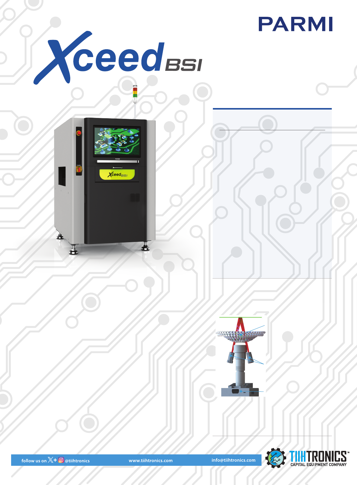
Bottom Side Inspection
‘Xceed BSI’ is a 2D & 3D AOI machine that inspects the bottom side of the PCB
without flipping the board after wave or selective soldering. Since it is not necessary
to flip the PCB, it eliminates unnecessary handling of the PCB and minimizes the
footprint of the line. The main uses of the machine are to inspect the condition of the
pins and solder joints after soldering of THD components. ‘Xceed BSI’ can also be
used for general SMD components inspection on the bottom side of the PCB.
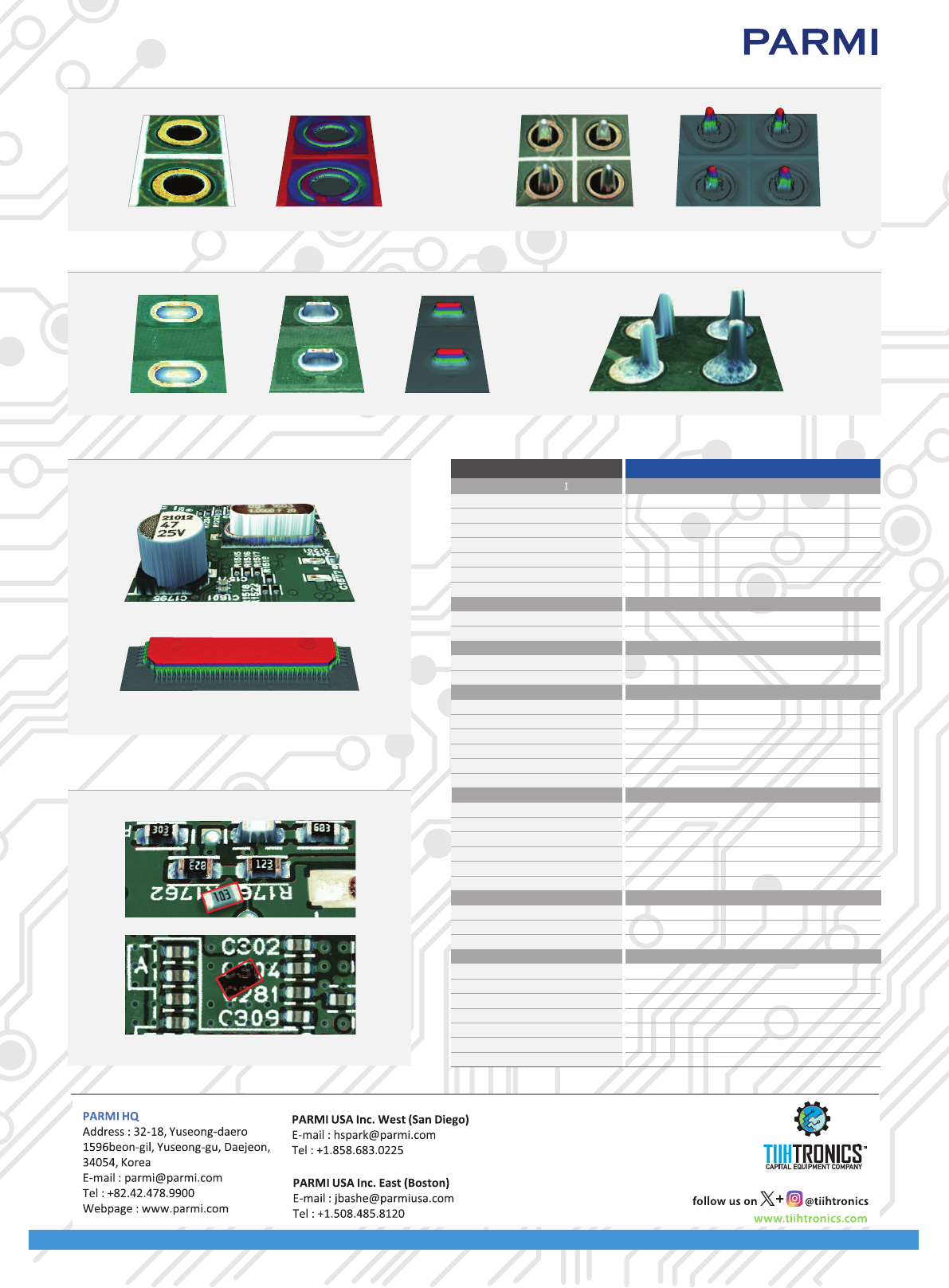
S
older joints generally have specular properties such as mirror surfaces. PARMI’s
3D sensor uses a highly focused laser beam to accurately measure the mirror-like
solder joints. In other words, based on actual data, not p
redictions or estimates, it
accurately detects true defects without false calls. Main inspection items are older
fillet shape (Area, Height), pin position and height. Separately, foreign material and
contamination existing on the PCB are inspected without increasing the cycle time.
In
addition, our exclusive dual laser technology provides the capability to inspect
components
and pins up to 35mm high with the same precision as small components.
‘Xceed BSI’ utilizes the same software environment and algorithms as the standard
Xceed machine. All programming can be performed in a consistent manner with the
SMD inspection processes by using the same teaching, operation and inspection,
verification, and SPC (Statistical Process Control) programs.
The precise sensor head driven by a linear motor minimizes the vibration of the
machine, and the robust conveyor safely handles
very heavy products. All hardware
including the laser sensor are selected, engineered, and built for durability to
ensure long MTBF and to minimize maintenance of the machine.
Bottom Side Inspector optimized for
THT Process
Key Features
•
3D AOI for bottom side inspection
•
Space saving by eliminating the need
for PCB flip unit
•
Primary inspection functions:
Wave or selective soldering including
THD pin position and height, and
solder joint inspection (Insufficient,
Excessive, Bridging, etc.)
•
Full inspection of mixed technology
PCBs (SMD & THD)
•
100% inspection of PCB warp and
foreign material with no cycle time penalty
•
Perfect inspection of mirror-like
solder joints by highly focused laser
sheet beam
7 Channel LED : Color 2D
PCB
Shadow Free Dual Laser : 3D
Ultra Fast 2D & 3D Sensor
Signal Processing by FPGA
PARMI MEXICO
WTCG Torres Corporativas
Av. Rinconada de las Praderas #1249 B-303
Col. Valle Verde C.P. 44550
Guadalajara, Jal. México
+52 81 1015 7866
www.parmi.com
info@tiihtronics.com
Specifications
Shadow Free Dual Laser Optical Triangulation
4M Image Sensor / Telecentric Lens
R.G.B LED 3 Stage Lightings
37
85
0.5
3 sigma < 3µm
5µm
±5 (2%)
35
1,030 × 1,405 × 1,573
700
860 ~ 970
300 ~ 800
Left to Right, Right to Left (Factory Setting)
Display
Inspection Program
Auto
SPC&Process Monitoring
Windows 7 or above
i7-7800X or above
Verification Program
AOIworks
ePM (Gerber, BOM, Cad)
24" Monitor
SPCworksAOI, xNetHub
Veriworks
Xceed BSI
Measuring Principle
Camera
Illumination
Scan Speed (sq.cm/sec)
Scan Width (mm)
16.7 × 16.7
X-Y Resolution (µm)
Height Resolution (µm)
Height Repeatability
Height Accuracy
PCB Warpage (mm)
Max. Component Height (mm)
Min. Size (mm)
Thickness (mm)
Top/Bottom Edge Clearance (mm)
Top/Bottom Clearance (mm)
W×D×H (mm)
Conveyor Height (mm)
Panel Flow Direction
Conveyor Width Adjusting
Vision Module : TRSC
-
Model
Max. Size (mm)
Operating System
Teaching Program
Weight (kg)
Barcode(1D/2D) Recognition
(Option) Offline Teaching Program
AOIManager, AOIDBManager
Built in AOIworks
AOIworks Offline
System Diagnosis
Performance
Measurement
Max. Weight (kg)
Conveyor Speed Range (mm/sec)
CPU
Panel Dimension
System Dimension
Computer & Console
Software
Specifications in this catalog are subjected to change without notice for quality improvement. Rev.2
General SMD
Foreign material / Contamination
Pin Inspection before Soldering
Solder Joint and Pin Inspection after Soldering
50 × 50
410 × 410
1 ~ 12
10
4 / 4.1
100 /
••••