q330-e1-05.pdf - 第2页
System Configuration Inspection Program Creation Terminal Ethernet v-DB v-TS Inspection Result Viewer Terminal v-CA Quality Improvement Support System Using Inspection Data Dedicated Database for Inspection System Q-up Sy…
Omron's 3D-SJI (Solder Joint Inspection)
Ensuring High-quality Products
in an Efficient Manufacturing Environment
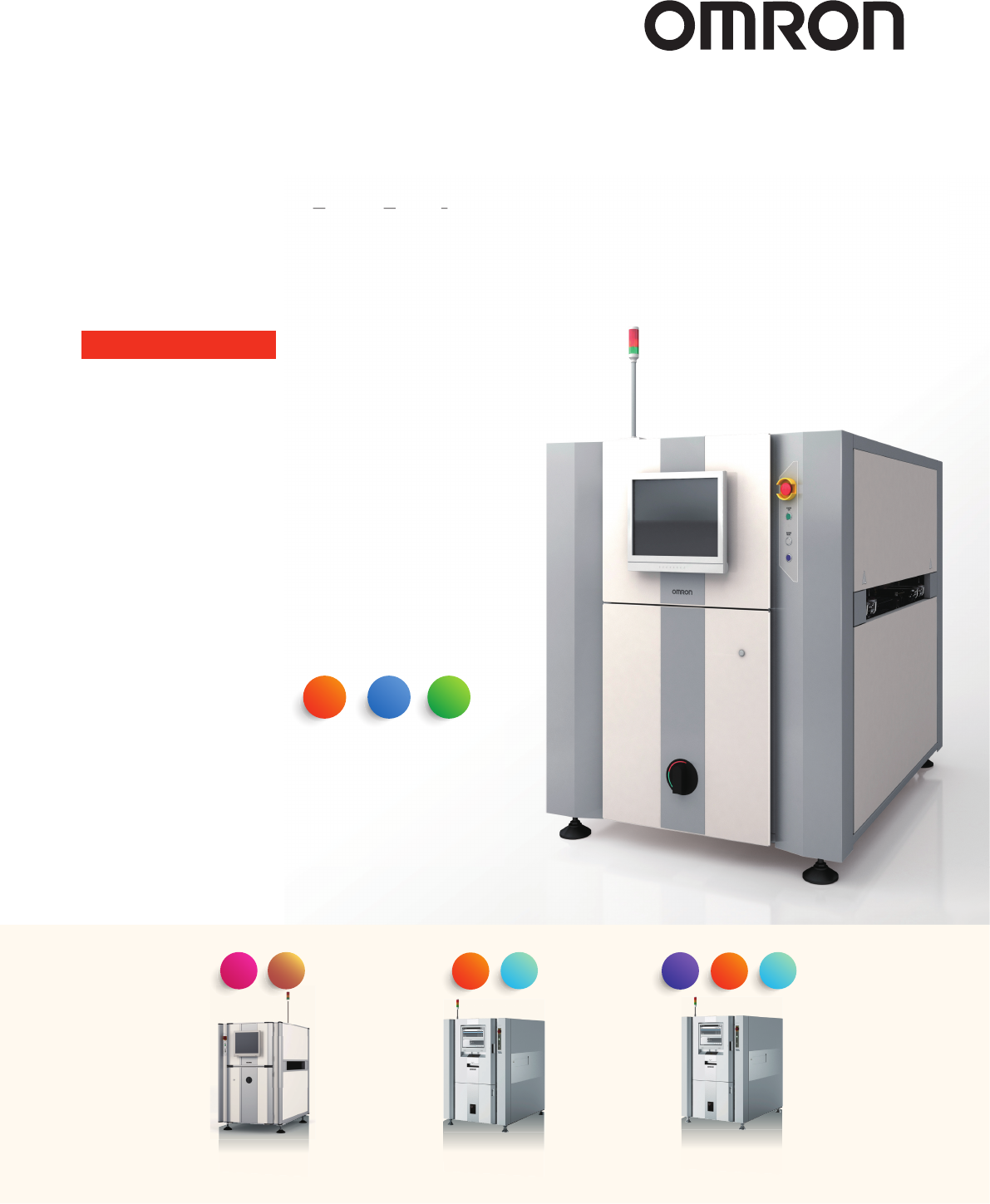
VT-S530
Advanced & High-speed
VT-S730-H
PCB Inspection System (AOI) Lineup
Best Sales in Automotive Industry
VT-S730
Hardware configuration
Dimensions
Weight
1180(W)×1640 (D)×1500(H) mm
Approx. 850kg
200 - 240VAC (single phase),
voltage fluctuation range ±10%
2.0kVA
900±20mm
0.3 - 0.6MPa
10 - 35°C
35 - 80%RH (Non-condensing)
12M pixel camera
3D reconstruction through color highlight and
phase shift technology
10μm/15μm
10μ: 40×30mm
15μ: 60×45mm
Dimensions
(Unit: mm)
(645 max.) 1640 (961 max.)
1500
±20
2000
88
±20
1180
±20
71 345 740
900 ±20
PCB Inspection System
VT-S530
3D
Dual
Lane
High
Resolution
High-Resolution Model
The information provided in this document is mainly for selecting a suitable model. Please read the Instruction Sheet carefully as it contains
information regarding warranty, limitations of liability, and precautions. Before purchasing, the user must understand and accept the information
presented in the Instruction Sheet.
This product may cause interference if used in residential areas.
Cat. No. Q330-E1-05
Note: Specifications subject to change without notice
OMRON Corporation
INDUSTRIAL AUTOMATION COMPANY
INSPECTION SYSTEMS BUSINESS DIVISION
SALES DEPARTMENT
Shinagawa Front Bldg. Conference 7F
2-3-13 Kounan Minato-ku Tokyo
108-0075 JAPAN
TEL +81-3-6718-3550 FAX:+81-3-6718-3553
OMRON INDUSTRIAL AUTOMATION
(
CHINA
)
CO., LTD.
TEL:
+
86-755-8359-9028 FAX:
+
86-755-8359-9628
Authorized Distributor:
OMRON ELECTRONICS LLC
2895 Greenspoint Parkway, Suite 200
Hoffman Estates, IL 60169 U.S.A
TEL:+1
-847-843-7900
FAX:+1
-847-843-7787
OMRON ELECTRONICS KOREA CO.,LTD.
21F, KyoboTower B Wing, 465, Gangnam-daero,
Seocho-gu, Seoul, Korea 137-920
TEL:
+
82-2-3483-7789 FAX:
+
82-2-3483-7788
0119-0.3M(0119)
Omron AOI Business Europe, Omron Europe B.V.
Zilverenberg 2, 5234 GM 's-Hertogenbosch, The Netherlands
TEL:
+
31 (0)736
-
481811 FAX:
+
31 (0)736
-
481879
OMRON ASIA PACIFIC PTE LTD
438A Alexandra Road #05-05/08 (Lobby 2)
Alexandra Technopark Singapore 119967
TEL:+65-6835-3011 FAX:+65-6835-2711
F20,TowerA,NEO Building,6011ShennanAvenue,
Futian District, Shenzhen, Guangdong
518048, China
Imaging system
Inspection principle
Image resolution
FOV
Voltage
Normal rated power
Image signal
input block
Line height
Air supply pressure
Operating temperature range
Operating humidity range
Power supply
Supported PCB size (min.)
Supported PCB size (max.)
Clearance
Height measurement range
Thickness
Inspection item
50(W)×50(D)mm
Dual lane: 510(W)×330(D)mm
Single lane: 510(W)×680(D)mm
Above: 50mm; Below: 50mm
25mm
0.4 - 4mm
Component height, lift, tilt, missing/wrong
component, wrong polarity, flipped component,
OCR inspection, 2D code, component offset
(X/Y/rotation), fillet (height/length, end joint
width, wetting angle, side joint length), exposed
land, foreign material, land error, lead offset,
lead posture, lead presence, solder ball, solder
bridge
Functional specifications
2D
Implement-
ation
Inspection
Oblique
View
3D
High-
Speed
Oblique
View
3D
Support for Post Placement
VT-S500
System Configuration
Inspection Program
Creation Terminal
Ethernet
v-DB
v-TS
Inspection Result
Viewer Terminal
v-CA
Quality Improvement Support
System Using Inspection Data
Dedicated Database
for Inspection System
Q-up
System
Whole PCB surface inspection
特徴パラメータ表示
特徴パラメータ編集
30
検査基準
検査項目 設定値
ー
ー
0
0
0.1
30
0.04
異物
長短径比(%)
面積(mm
2
)
■高さ(mm)
Foreign object (0402 scattered chip)
detection example
High production throughput supported through dual lane.
Dual lane
operation using various PCBs is possible, due to its handling
capability up to the PCB size of 510 (W) x 330 (D) mm.
High productivity inspection
Example Defects
Reduction of man-hours required
for initial program creation.
Hybrid
* IPC quality standard is adopted
Threshold Setting
Fillet Width
Fillet Length
Fillet Height
Direct input of quality
product criteria
Omron's 3D-SJI S SeriesOmron's 3D-SJI S Series
Automation has reduced man hours required for initial program
creation time. Quantitative "quality criteria" based on 3D
reconstruction has substantially reduced man hours required for
debugging.
Traditional modelsTraditional models
Continuous adjustment is required with each lot
fluctuation or new defect occurrence. This model
requires continuous debugging.
Contributing to quality control that conforms to International Standards, including IATF (ISO/TS) 16949.
1
POINT
2
POINT
3
POINT
Lifted micro component (0603) defect
Microscope image Quantitative inspection
Reconstructed 3D image
Microscope image Quantitative inspection
Reconstructed 3D image
Micro component (0603) insufficient solder wetting defect
Micro component (0402) offset defect
Microscope image Quantitative inspection
Reconstructed 3D image
Microscope image Quantitative inspection
Reconstructed 3D image
Micro component (0402) inclination defect
Insufficient solder
Flow solder/insertion component inspection examples
Excess solder Lead height defect
Micro solder ball inspection example
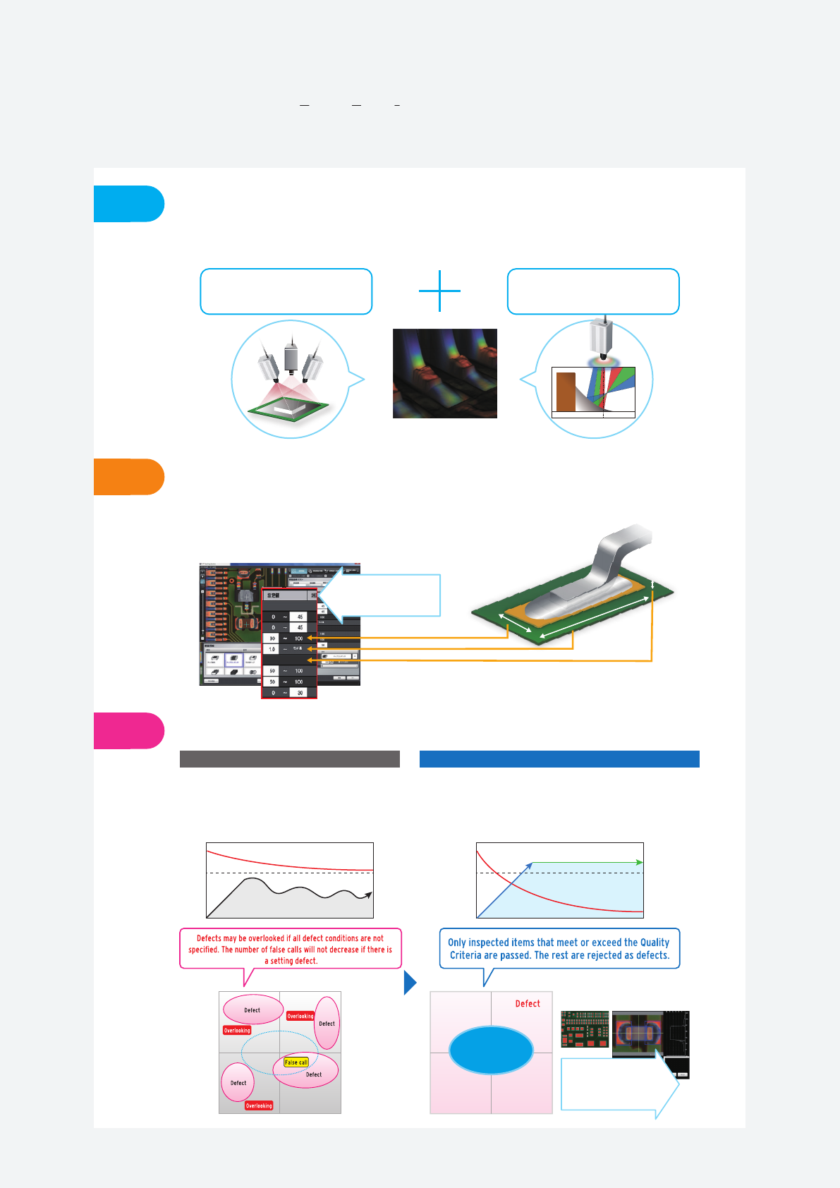
Omron's 3D-SJI
(Solder Joint Inspection)
Materializes quantitative inspection of solder joint and implementation, while minimizing risks of overlooking
unknown defects by the quality product criteria inspection based on the standards, contributing to vertical startup of
inspection.
Conducts optimal inspection to suit items to be inspected by combining 3D and 2D technologies.
3D reconstruction of solder and components
Hybrid 3D-SJI
Phase-shift principle
suitable for height measurement
Color highlight
to capture the shape without being
affected by the solder surface state
Quantitative inspection utilizes quality criteria based on
International Standards*
Materialization of maximum quality inspection with minimum man-hour
Required inspection quality
Quality fluctuation
Difficult to reduce man-hours
Sustaining Stable Inspection
Vertical Startup
Required inspection quality
Reduction of
man-hours
Pass
Lands are automatically
extracted from a bare board
and Component Windows are
auto-generated based on the
height information.
VT-S530
Detecting foreign objects accurately is achieved through combining
3D (height) and 2D (area) measurements on the entire PCB surface.
(Lands without solder can be excluded from the inspection)
Detection
sensitivity can be
easily adjusted
by the slider
Omron's "Quality Criteria"Traditional
System Configuration
Inspection Program
Creation Terminal
Ethernet
v-DB
v-TS
Inspection Result
Viewer Terminal
v-CA
Quality Improvement Support
System Using Inspection Data
Dedicated Database
for Inspection System
Q-up
System
Whole PCB surface inspection
特徴パラメータ表示
特徴パラメータ編集
30
検査基準
検査項目 設定値
ー
ー
0
0
0.1
30
0.04
異物
長短径比(%)
面積(mm
2
)
■高さ(mm)
Foreign object (0402 scattered chip)
detection example
High production throughput supported through dual lane.
Dual lane
operation using various PCBs is possible, due to its handling
capability up to the PCB size of 510 (W) x 330 (D) mm.
High productivity inspection
Example Defects
Reduction of man-hours required
for initial program creation.
Hybrid
* IPC quality standard is adopted
Threshold Setting
Fillet Width
Fillet Length
Fillet Height
Direct input of quality
product criteria
Omron's 3D-SJI S SeriesOmron's 3D-SJI S Series
Automation has reduced man hours required for initial program
creation time. Quantitative "quality criteria" based on 3D
reconstruction has substantially reduced man hours required for
debugging.
Traditional modelsTraditional models
Continuous adjustment is required with each lot
fluctuation or new defect occurrence. This model
requires continuous debugging.
Contributing to quality control that conforms to International Standards, including IATF (ISO/TS) 16949.
1
POINT
2
POINT
3
POINT
Lifted micro component (0603) defect
Microscope image Quantitative inspection
Reconstructed 3D image
Microscope image Quantitative inspection
Reconstructed 3D image
Micro component (0603) insufficient solder wetting defect
Micro component (0402) offset defect
Microscope image Quantitative inspection
Reconstructed 3D image
Microscope image Quantitative inspection
Reconstructed 3D image
Micro component (0402) inclination defect
Insufficient solder
Flow solder/insertion component inspection examples
Excess solder Lead height defect
Micro solder ball inspection example
Omron's 3D-SJI
(Solder Joint Inspection)
Materializes quantitative inspection of solder joint and implementation, while minimizing risks of overlooking
unknown defects by the quality product criteria inspection based on the standards, contributing to vertical startup of
inspection.
Conducts optimal inspection to suit items to be inspected by combining 3D and 2D technologies.
3D reconstruction of solder and components
Hybrid 3D-SJI
Phase-shift principle
suitable for height measurement
Color highlight
to capture the shape without being
affected by the solder surface state
Quantitative inspection utilizes quality criteria based on
International Standards*
Materialization of maximum quality inspection with minimum man-hour
Required inspection quality
Quality fluctuation
Difficult to reduce man-hours
Sustaining Stable Inspection
Vertical Startup
Required inspection quality
Reduction of
man-hours
Pass
Lands are automatically
extracted from a bare board
and Component Windows are
auto-generated based on the
height information.
VT-S530
Detecting foreign objects accurately is achieved through combining
3D (height) and 2D (area) measurements on the entire PCB surface.
(Lands without solder can be excluded from the inspection)
Detection
sensitivity can be
easily adjusted
by the slider
Omron's "Quality Criteria"Traditional