CM602规格说明书(英文).pdf - 第25页
CM602-L 2006.0515 - 20 - 4.3 Recognition Unit Configuration ■ Line Camera The pos ition in pick ing up t he chip a nd the ang le de viation are corr ected with the im age of line c amer a. In additio n, the pres ence of …
CM602-L 2006.0515
- 19 -
■
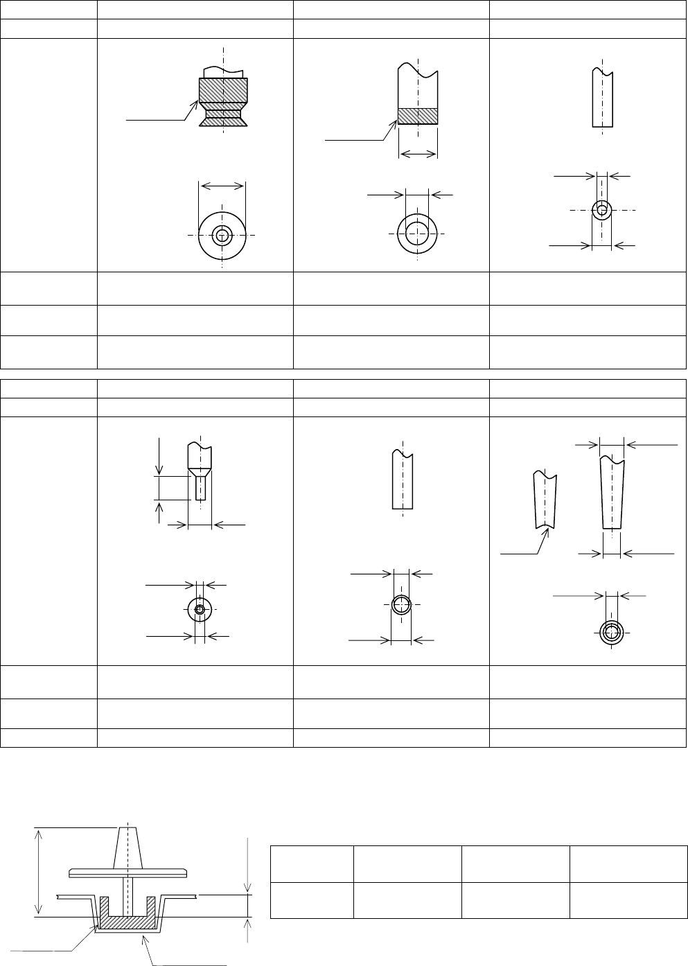
Nozzle for chip components / QFP
∗
The product number should be used for order placements. (Unit: mm)
Nozzle No. 1403 1479 1514
Product number
KXFX0556A00 KXFX05ASA00 KXFX05G9A00
Nozzle unit
shape
(Unit: mm)
Target
component
QFP QFP Volume
Max. component
height
21 mm 18.5 mm 21 mm
Remarks
With a urethane pad
Nozzle length: 22.5 mm
With a urethane rubber
Nozzle length: 27.5 mm
Nozzle length: 22.5 mm
Nozzle No. 1518 1580 1604
Product number
KXFX05GHA00 KXFX05KRA00 KXFX05L9A00
Nozzle unit
shape
(Unit: mm)
Target
component
Terminal LED
Melf
Φ
2.2
∼
Φ
2.5
Max. component
height
21 mm 21 mm 21 mm
Remarks Nozzle length: 22.5 mm Nozzle length: 22.5 mm Nozzle length: 22.5 mm
■
Correspondence between the pickup depth of electronic component and the nozzle length
The necessary nozzle length varies according to the pickup depth (distance from top of embossed tape to
pickup surface) of electronic component to be placed.
Pickup
depth B
0 mm
to below 3 mm
3 mm
to below 8 mm
8 mm
to below 13 mm
Nozzle
length A
22.5 mm 27.5 mm 32.5 mm
Pad
φ
6
φ
6
Urethane
rubber
φ
5
φ
3
φ
1.2
φ
2.5
φ
2
φ
2.5
φ
3
3.1
φ
0.9
φ
1.2
R1.25
φ
1.6
φ
2.2
φ
3
Emboss tape
Component
Nozzle
length A
Pickup
depth B
CM602-L 2006.0515
- 20 -
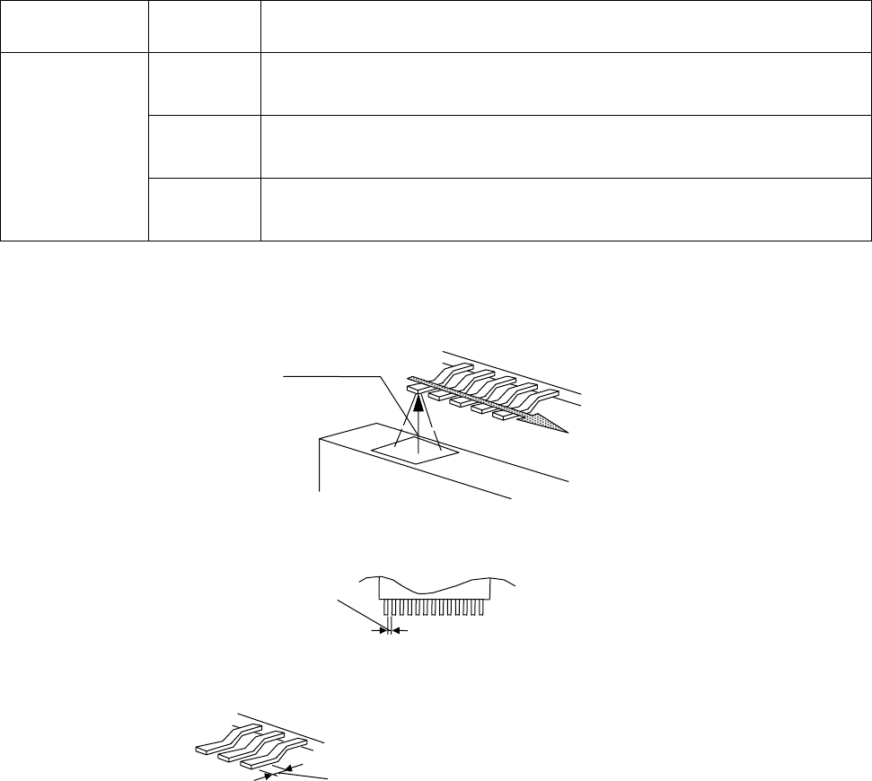
4.3 Recognition Unit Configuration
■
Line Camera
The position in picking up the chip and the angle deviation are corrected with the image of line camera.
In addition, the presence of solder bumps can be detected
(*)
for BGA/CSP through the side lighting (option).
* There are limitations on the chips for which the bump detecting feature is available.
Please see the items describing the recognition condition of BGA.
Recognition
method
Recognition
speed
Applicable Component
Low
Components with leads of 0.5 mm or less pitch, and CSP.
Middle
BGA and 0603 (0201”) chip.
Chip with leads of the pitch between 0.5 mm and 0.8 mm.
Batch
recognition
High
General chip components including the square chips measuring 1005
(0402”) or over.
■
Lead Checker (Option)
Floating leads are detected by laser scanning all the leads of SOP, QFP, etc. whose size is 50 mm × 50 mm
or less.
・
Measurable range of the floating lead is up to ±0.75 mm.
・
Lead opening must be 0.2 mm or over to be detected.
・
Lower plane of the lead must be 0.2 mm or over to be detected.
・
Some leads cannot be laser scanned depending on the state of the leads’ bottom.
So please consult us before adopting this option.
■
PCB Recognition Camera
・
Visual field: 5 mm × 5 mm
(For information about the dimensions of PCB recognition mark, see “6. PCB Design Standards.”)
Lead checke
r
Laser light
Opening is 0.2 mm or over.
Lower plane of the lead is 0.2 mm or over.
CM602-L 2006.0515
- 21 -
■
Recognition conditions of QFP
Placement conditions of QFP are as follows.
(Basically, placement QFP is determined and experimented after getting the sample of it, and then it is
judged to be placed or not.)
High Speed head (8 nozzles) Multi-functional head
Outside dimensions 5 mm × 5 mm to 24 mm × 24 mm 5 mm × 5 mm to 45 mm × 45 mm
Thickness 1.0 mm to 6.5 mm 1.0 mm to 21 mm
Lead pitch 0.65 mm, 1.0 mm, 1.27 mm, 1.5 mm
0.4 mm, 0.5 mm, 0.65 mm,
1.0 mm, 1.27 mm, 1.5 mm
Lead width 0.2 mm or over
Lead shape Leads must be protruding out of the mold area by 1 mm or over.
・
Feeding type
Fed by tape.
Fed by tray (supported by the shuttle tray feeder (option) or the direct tray feeder (option)).
* For information about the components that are not conforming to the above specifications, please consult us.
■
Recognition conditions of BGA
Placement conditions of BGA are as follows.
(Basically, placement BGA is determined and experimented after getting the sample of it, and then it is judged
to be placed or not.)
High Speed head (8 nozzles) Multi-functional head
Outside dimensions 7 mm × 7 mm to 24 mm × 24 mm 7 mm × 7 mm to 45 mm × 45 mm
Thickness 1.0 mm to 6.5 mm 1.0 mm to 21 mm
Bump pitch 1.0 mm, 1.27 mm, 1.5 mm
Bump diameter
φ
0.5 mm,
φ
0.7 mm,
φ
0.9 mm
Bump shape Globular, cylindrical, or lead form
Materials of bump High temperature solder, eutectic solder, 42 alloy lead
Number of bumps Matrix of Min. 3 × 3 to Max. 50 × 50
Arrangement of
bump
The pitch and dimensions of bump shall be consistent.
The bump missing and the staggered pattern are the same as those defined by
JEDEC and EIAJ regarding BGA.
・
To enable the simultaneous recognition of BGA appearance and solder balls, the body shall be made of
the glass epoxy. The recognition depends on the conditions of the placement surface of solder balls (pat-
tern, with or without through hall, luster, etc.).
・
BGA which is made of ceramic and has the gold body is placed with only the contour recognition.
・
Surface of bump
The surface of bump should be free from the blur due to oxidation.
(It needs to be checked whether to recognize or not, according to the condition of oxidation.)
・
Feeding type
Fed by tape.
Fed by tray (supported by the shuttle tray feeder (option) or the direct tray feeder (option)).