FuzionSC_Platform_brochure.pdf - 第2页
Build better. Build more. Spend less. Empowered by know-how Universal Instruments’ solutions include not only best-in-class equipment, but also proven in-depth process knowledge, applica- tion expertise and integration e…
www.uic.com
email: universal@uic.com
AMERICAS
Tel. 1-800-432-2607 or
Tel. +1-607-779-7522
CHINA, SHENZHEN
Tel. +86-755-2685-9108
CHINA, SHANGHAI
Tel. +86-21-6495-2100
EUROPE
Tel. +421-2-4930-96-60
©2019 Universal Instruments Corporation.
All rights reserved. All specications are
subject to change.
MC-6454A 08/19
semiconductor performance
at surface mount speeds
Build better. Build more. Spend less.
Empowered by know-how
Universal Instruments’ solutions include not only best-in-class
equipment, but also proven in-depth process knowledge, applica-
tion expertise and integration experience to ensure your equipment
delivers your product at the highest possible yield and reliability, and
at the lowest possible cost.
Achieve best accuracy at highest speed over largest area
• ±10µm accuracy, < 3µm placement repeatability
• High throughput up to 10K cph Advanced Packaging Assembly
Solutions (APAS), 30K cph standard applications
• Populate the largest panels to process higher die counts
All-in-one platform for any assembly challenge
• Place broad range of die and components on one platform
• Placement capability from ANY feeding option
• Place on ANY substrate
Leverage process expertise and years of experience
• Advanced Process Lab focused on realizing rapid product
introduction, maximizing yield and optimizing reliability
• APAS applications since 1990; thousands of platforms, all markets
System-level solutions for next-generation challenges
Bringing high productivity to advanced packaging assembly
Traditional advanced assembly methods can no longer keep pace with today’s
higher-volume, higher-complexity production demands. Universal’s FuzionSC™
Platform oers a complete solution to today’s most challenging semiconductor
packaging applications by combining extreme accuracy with surface mount
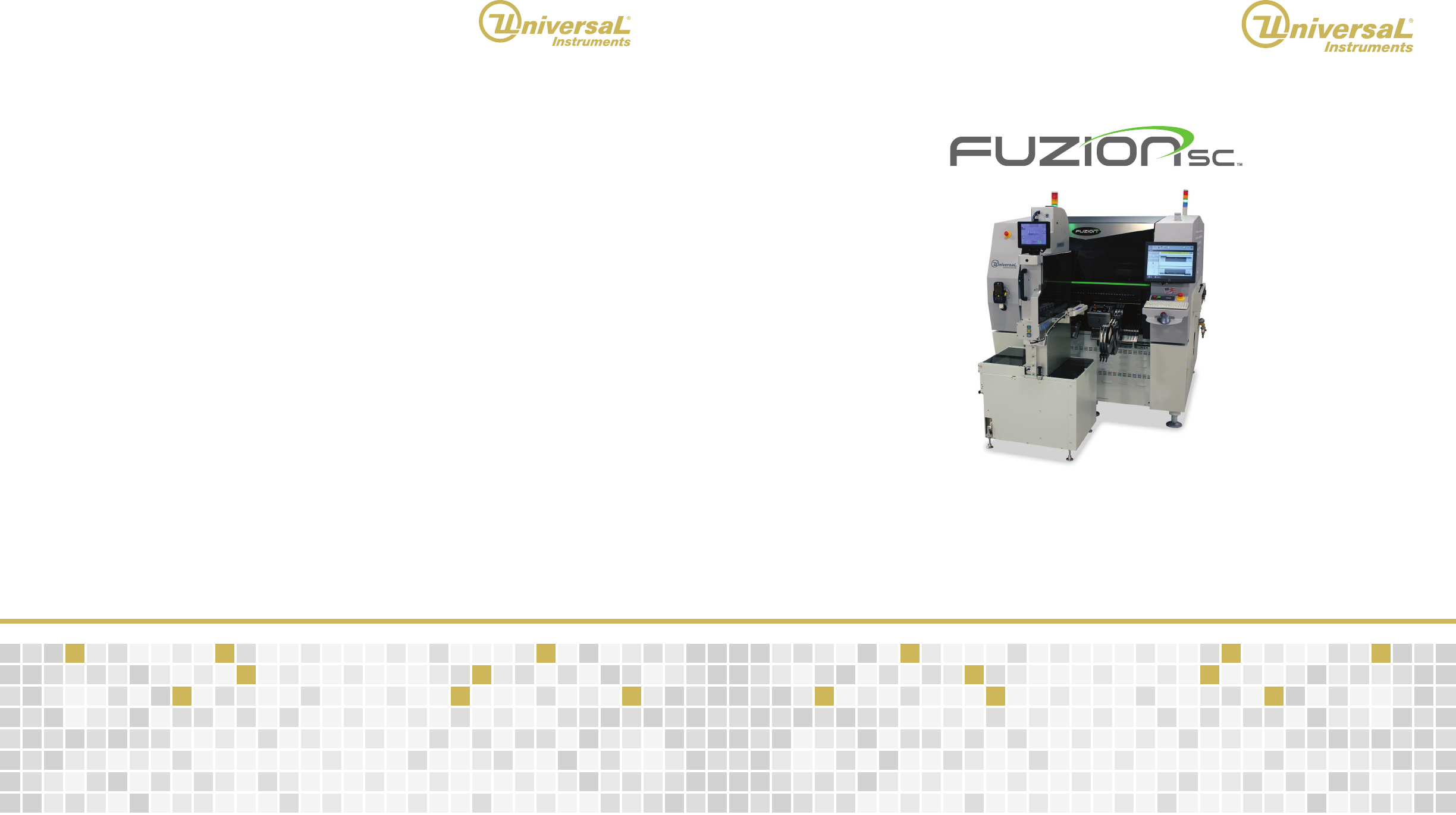
performance. FuzionSC is the ideal solution for Flip Chip, System-in-Package (SiP),
2.5D, Package-on-Package (PoP), Wafer and Panel-level Fan-out, Embedded, and
Conformal Shielding applications.
With the largest component range of any advanced packaging pick-and-place solu-
tion, FuzionSC has the inherent capability to assemble a complete module on a single
machine, placing both die and passives precisely and seamlessly. This enables you to
move quickly and cost-eectively to your next product while getting to market faster,
minimizing operating costs and enjoying long-term asset protection.
Building Better
New Benchmark
Achieve best accuracy at highest speed over largest area
±10µm accuracy, < 3µm placement repeatability
• High-stiness frame, within 1µm from corner to corner
• Proprietary VRM linear motor: thermally stable, dual-drive, 1µm resolution
• Optimized motion control for sub-micron repeatability
• Environmental thermal management
• High-resolution optics, mapping and calibration routines
• Two-step precise global ducial nd
• Look before pick
• Top Alignment Process (TAP)
• Accuracy Management System (AMS) validates accuracy while in production
• AOI feedback and placement adjustment
High throughput up to 10K cph APAS, 30K cph standard applications
• Dual-drive VRM linear motor with fast motion response and settling times
• Available dual-beam congurations with multiple heads
• Multiple heads/spindles reduces number of cycles from pick to place
• Gang pick and gang dip maximizes cycle time eciency
• On-the-y vision with large eld of view
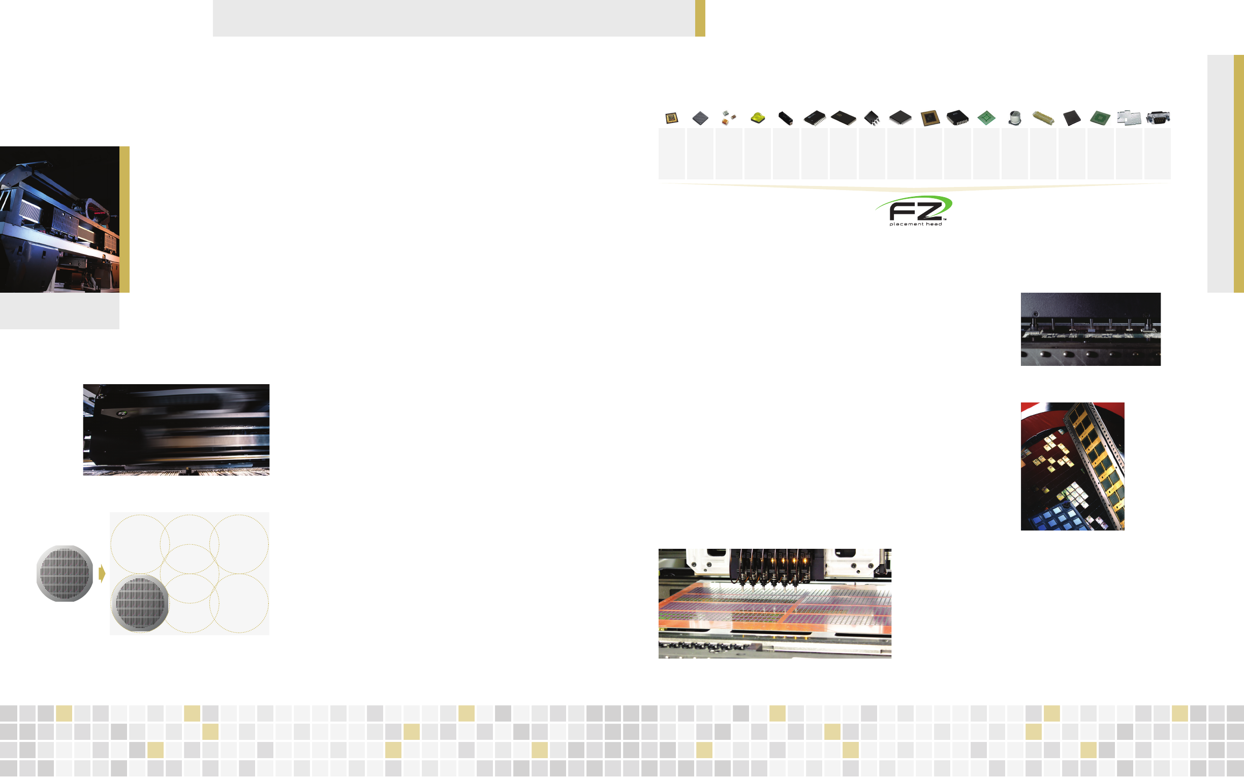
Populate the largest panels to process higher die counts
• Traditional platforms follows wafer form factor, limiting assembly size
• Populate panels without sacricing speed or accuracy
• Achieve a 7X processing increase!
300mm
~71K mm
2
625mm x 813mm
~508K mm
2
All-in-one platform for any assembly challenge
Place broad range of die and components on one platform
• High-accuracy ip chip, bare die, surface mount, and odd-form
• Full range of die: 0.5–40mm, 0.05–4mm thick
• Advanced vision algorithms, programmable lighting, bump recognition down to 20µm
• SMT: 01005–55mm square and up to 25mm tall
• Supports solder/ux dipping and pin transfer
• 150–5000g placement force (lower-force options available), dynamic force control
Placement capability from ANY feeding option
• Wafer, tray, tape, tube, and bulk
• Supports wafers up to 300mm and multiple die part numbers
• Tape: 4 x 1mm (01005) up to 56mm
• Matrix tray: supports stationary and automated stackable feeders (2x2, 4x4, JEDEC)
All-Around Performer
Place on ANY substrate
• Thin, thick, narrow, and large assembly area
• Substrates, wafers, lead frames, ceramics, glass, ex, and laminates
• Reel-to-reel systems
Bare Die
Flip Chip
Chip
LED
Tant Cap
SOIC
TSOP
DPAK
QFP
BGA
PLCC
CSP
Electrolytic Cap
Connectors
CCGA
BNGA
Odd-Form
Pin-in-Paste