SJ411DCB1-02E_mail.pdf - 第2页
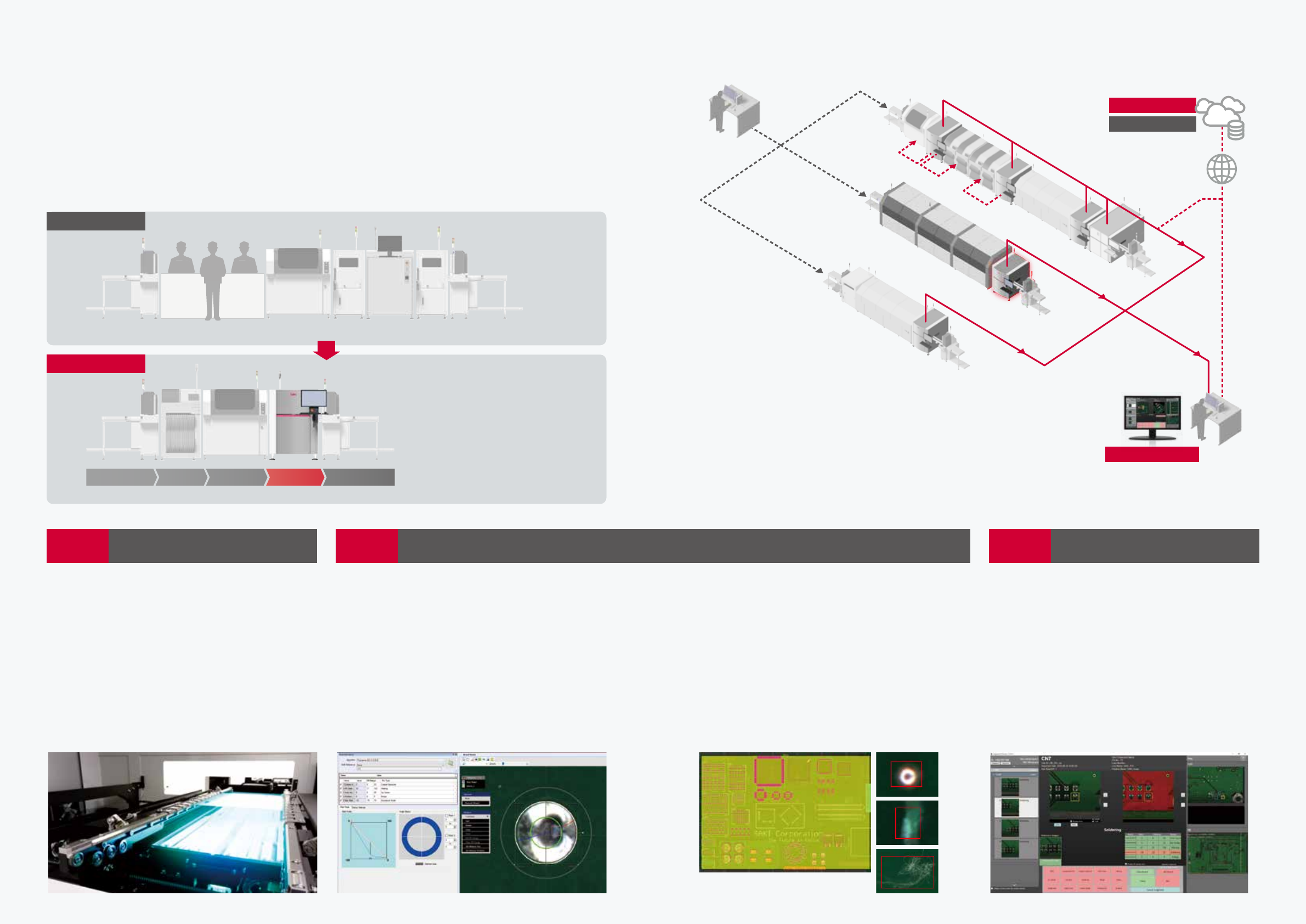
3D AOI 3D SPI 3D AOI 2Di-LU1 Coating AOI Judgement Station SPC & Report MES & ERP Internet Cloud-based Management System Feed Forward Feed Back Feed Back 3D AXI 2 3 Bottom- sc an AOI s ys tem for automated PCB ba…
Inline Bottom-side 2D Automated
Optical Inspection System
2Di-LU1
Back-end inline solution after selective
and wave soldering
Model Name 2Di-LU1
Resolution 18 µm
Target PCB Size
mm (in.)
Carrier:
50 W x 60 L - 610 W x 610 L mm
(1.97 W x 2.36 L –24.02 W x 24.02 L in.)
Inspection area (Scan):
50 W x 60 L - 460 W x 500 L mm
(1.97 W x 2.36 L –18.11 W x 19.69 L in.)
PCB Thickness 0.5 - 5.2 mm (0.02-0.20 in.)
PCB Weight 12 kg (26.46 lbs) or less
PCB Clearance
Top: 130 mm (5.12 in.),
Bottom: 40 mm (1.57 in.)
Heat Resistant
Temperature
70°C (158F) or lower
Inspection
Categories
Solder inspection for THT (Copper, Blow Hole,
Pin, Fillet, Absence of Solder, Bridge)
*Each defect name can be arranged freely by
the system function
Transfer Conveyor
Method
Flat belt transfer
Transfer Conveyor
Height
880 - 965 mm (34.65 - 37.99 in.)
Operating System
Windows 10 IoT Enterprise 64 bit
English Editon (Microsoft)
Electric Power
Requirement
~ 200 - 240V +/-10%, 50/60Hz, 700VA
Air Requirement 0.5MPa, 5L/min (ANR)
Usage Environment
15°C (59F) - 30°C (86F) / 15 - 80% RH
(Non-condensing)
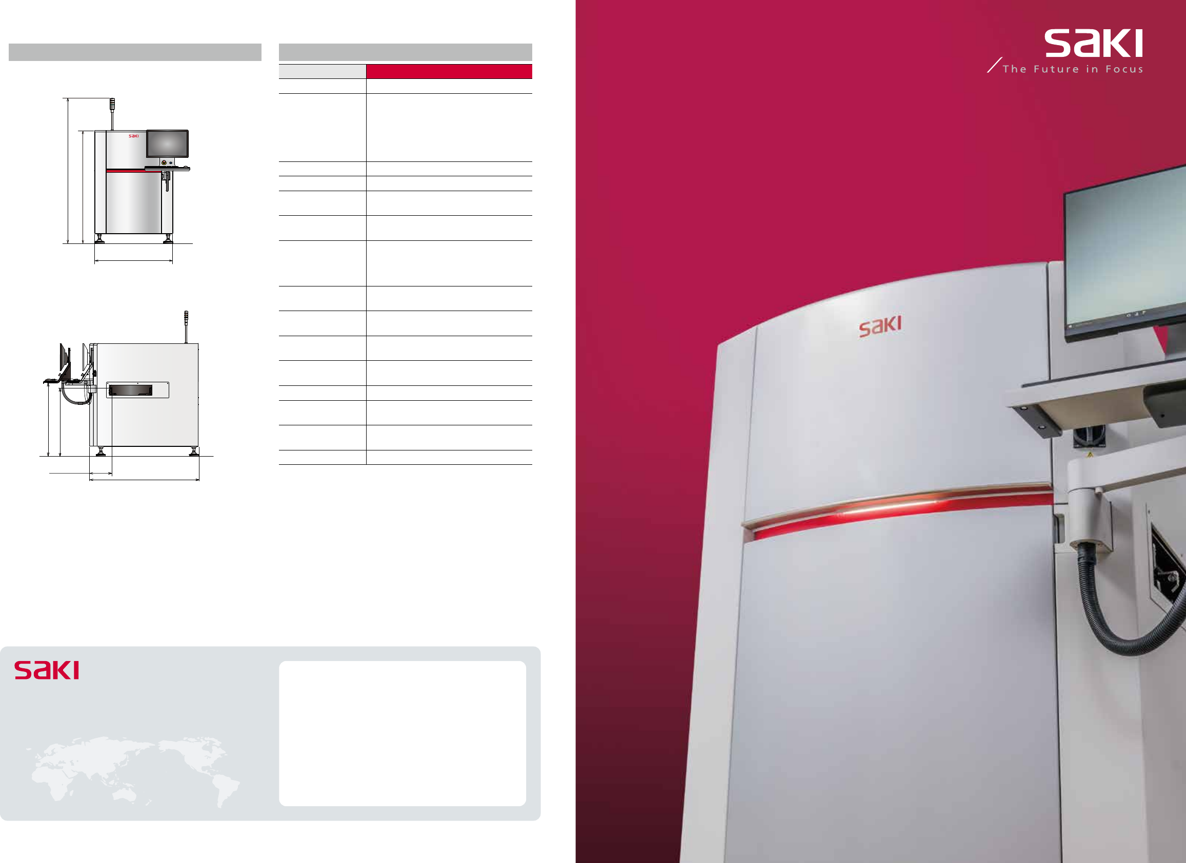
Dimensions
W x D x H(Main body)
1040 x 1440 x 1500 mm
(40.94 × 56.69 × 59.06 in.)
Weight Approx. 750 kg, 1653.47 lbs
Dimensions Hardware / Function Specifications
■
Front View (mm, in.)
■
Side View (mm, in.)
Global Network
https://www.sakicorp.com/en/
Headquarters
DMG MORI Tokyo Digital Innovation Center
3-1-4, Edagawa, Koto-ku, Tokyo, 135-0051, Japan
TEL: +81-3-6632-7910 FAX: +81-3-6632-7915
Saki Corporation
(345, 13.93)
1440, 56.70
(1000, 39.37)
(900, 35.44)
1040, 40.94
(1500, 59.05)
(1930, 75.98)
© 2021 Saki Corporation. All Rights Reserved.
Specifications contained in this flyer are subject to change without notice.
Flyer Version: June 2021
SJ411DCB1-02E
3D AOI
3D SPI
3D AOI
2Di-LU1
Coating AOI
Judgement Station
SPC & Report
MES & ERP
Internet
Cloud-based
Management System
Feed Forward
Feed Back
Feed Back
3D AXI
2 3
Bottom-scan AOI system for automated PCB back-end production.
Ensure full traceability and Quality Assurance Data availability for back-end production.
Prevent damage from manual or automated board handling by eliminating the need to flip the PCBs.
SAKI Line Scan technology
SAKI’s unique Line Scan imaging technology is applied to bottom-side
inspection. High-speed imaging enables inspection of large PCBs
in one pass in about 9 seconds. The newly developed high-rigidity
conveyor is compatible with large odd-shaped inserted component
mounted-PCBs and heavy jigs. Covering the scanner with tempered
glass protects it against falling flux and foreign substances.
It provides easy maintenance and cleaning.
• Maximum PCB size 460 x 500 mm
(18.11 x 19.69 in.)
• Maximum PCB weight 12 kg (26.46 lbs)
• PCB clearance Top: 130 mm (5.12 in.), Bottom: 40 mm (1.57 in.)
Proven inspection algorithms
The highly rated FUJIYAMA algorithm provides through-hole
solder joint and pin inspection. By analyzing solder meniscus
and pin presence using SAKI’s unique lighting technology, the
following defects are simultaneously inspected:
• Copper exposure • Excessive solder
• Pin presence • Insufficient solder
• Blow holes • Solder bridges
Extra Component Detection (ECD) inspection capability
SAKI’s Line Scan technology scans the entire PCB in one pass.
By applying the ECD function, unexpected defects such as the
following can be detected automatically:
• Plastic mold chipping • Dropped chip parts
• Reel tape fragments • Foreign substances
• PCB pattern defects • Solder frame damage
Stable inspection performance
The introduction of the optical inspection system eliminates
inconsistencies in manual inspection quality, thereby maintaining
high quality inspection performance at all times.
Scalable and flexible design
To support diverse customer production requirements, SAKI offers a
highly scalable hardware/software design that is easy to integrate into
production management systems and production lines.
BF2 Integration
The new THT AOI adopts the same software platform as the 3D
Solder Paste Inspection machine (SPI) and 3D Automated Optical
Inspection machine (AOI) systems.
• Simple and easy user interface
• Effective defect judgement display
• Offline programming
• Statistical processing of inspection results
Additionally, by using the same system options as SAKI’s SPI and AOI
solutions, the operator’s workload is reduced. Maintenance is easy and
cost efficient since the same maintenance and service parts are used.
Key
Factor 1
SAKI's Proprietary Hardware
Key
Factor 3
SAKI QUALITY DRIVEN
Production Solution
Key
Factor 2
SAKI’s Unique Software
Bottom-side automated inspection machine for PCB back-end production SAKI QUALITY DRIVEN Production Solution
Ensuring the quality of through-hole solder parts after dip,
selective, and wave soldering, and improving productivity.
Solder
ball
Scratch
Fiber
Bottom-side AOI
2Di-LU1
Loader UnloaderSolderingAuto Insertion
TOP side AOILoader UnloaderSoldering Flipper Flipper
Conventional systems
2Di-LU1
Manual Insertion
Ensures quality and
productivity by eliminating
the need for manual
operation and board
flipping.
FUJIYAMA user interfaceBottom-side scanning ECD inspection window BF2-Monitor Image