Brochure-PacTech-Solder-Jetting-Laser-Bonding.pdf - 第2页
1 2 T urnkey Chemical Supplies • Al&CuPadCleaning • AlandCuPadActivation • ElectrolessNi,Pd,Ag,Cu • ImmersionAu&Ag • CyanideorCyanide-Free • SpecialSolutionsforNi&AgPad Cleanin…
Advanced Packaging Equipment
Solder Jetting & Laser Bonding
www.pactech.com
1 2
Turnkey Chemical Supplies
• Al&CuPadCleaning
• AlandCuPadActivation
• ElectrolessNi,Pd,Ag,Cu
• ImmersionAu&Ag
• CyanideorCyanide-Free
• SpecialSolutionsforNi&AgPad
Cleaning/Activation
• Photoresists&Solvents
Our mission is to reshape conventional soldering fundamentals with our contactless and stress-free
solder jetting technology. Our innovation radically supports the manufacturing needs by continuously
evolving into dierent applications.
PacTech – Packaging Technologies
Laser solder jetting technologies since 1995
Wafer Level Packaging
Services
• WaferFrontSidePlating
(electroless plating & electroplating)
• SolderBallAttach
• WaferBacksideMetallization
• WaferRepassivation
• WaferThinning&Dicing
• Otherbackendprocesses
Advanced Packaging
Equipment
• SolderJetting
• SolderReballing
• Soldering&WireBonding
• WaferLevelSolderBalling
• LaserBonding&Assembly
• ElectrolessBumpingLine
• CustomizedEquipmentfor
Photovoltaic&SolarIndustry
Assembly
OUR PRODUCTS AND SERVICES
1
SB
2
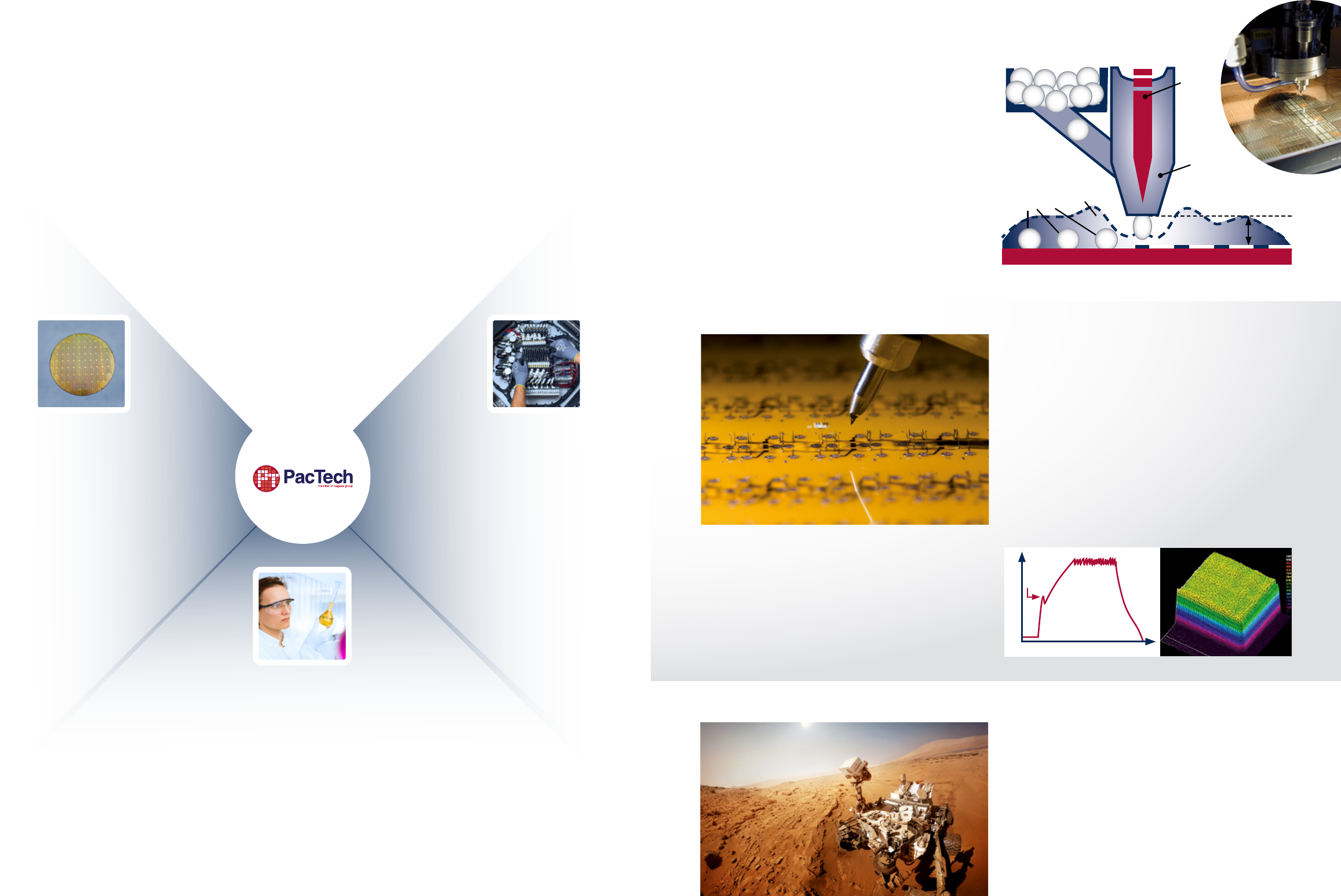
- Laser Solder Jetting
Our laser solder jetting technology is clean, precise, and
exible. The singulation disc will dispense a single solder
ball into the capillary where the laser beam’s thermal ener-
gy melts the solder ball, enabling it to fall onto any solder
position and being reowed immediately. It works with var-
ious solder alloys of dierent melting point and requires no
ux therefore it is clean.
The localized heat and short pulse generated by the laser
assures that minimal thermal stress is applied on the area
beyond the joined surfaces. The single solder ball dispens-
ing mechanism requires no tooling, hence enables exible
soldering location and contactless soldering.
LAPLACE – High Accuracy Placement
and Laser Bonding
Using localized laser heating mechanism, temperature
can be applied selectively in the interconnection areas of
interest without heating up the entire substrate up to the
reow temperature to liquefy and reow an interconnection
of a few microns. With customized bond tool and laser
technology, pick-and-place and assembly reow heating
are accomplished in single step at high accuracy < 5 µm.
Localized heat ensures reliable bonding of large dies while
the in-situ reow supports ultra-small die assembly as
small as 300 µm.
Our unique temperature control mechanism protects
single chip or component from being over-heated and
prevents substrate from warpage and repeating reow
circumstances.
Technology trendsetter in laser solder
jetting over two decades and still growing…
Being the leader in laser solder jetting, our technology has
been introduced into a wide array of applications includ-
ing industrial, medical, automotive, aerospace, and others.
Our innovative specialists have been working closely with
dierent industries to realize new applications and to con-
tribute in future development like we always do.
TEMPERATURE
TIME
Soldering
process
Laser
Capillary
Ball Reservoir
Reowed
solder balls
N
2
gas
Bond level
Bond padSubstrate
In-situ Laser Temperature Control & Beam Homogenization
PacTech’s solder jetting technology supports mission in outer space
3 4
High Accuracy Volume Manufacturing
SB² - Jet
Dimension
1262 x 987 x 1845 mm
Workspace
320 x 320 mm
Solder Ball Speed
6 - 8 balls / s
Solder Ball Ø
≥ 40 µm
Accuracy
+/- 3 - 5 µm (1 sigma)
Work Station
Chuck / Tray
Automation
Wafer handler, inline conveyor, JEDEC tray, others
Laser Man. Alignment
–
Laser Auto Alignment ü (3D)
Pattern Recognition
ü
2D Applications
ü
3D Applications
ü
Repair
optional
Products
Wafer pieces, PCB & Flex substrates, single chips, BGAs, CSPs, camera modules,
sensors, Hard Disk Drivers, 3D components, medical applications
Applications Technical Specications
Model
SB²-Jet
SB²-Jet:
Flagship platform of PacTech’s leading edge solder jetting
technology, the SB²-Jet with the high precision gantry is
the most advanced system for automated high-speed se-
quential solder ball attach and laser reow. With accurate,
precise and reliable performance proven in mass volume
production environment, the large working area of this
model is highly exible for a variety of dierent microelec-
tronic substrates and applications.
Hard Disk Drive
Assembly
3D Solder Jetting for
Optoelectronics
A comprehensive version of the SB²-Jet is delivered with
a vision and pattern-recognition system, an after-bump 2D
inspection and an additional repair unit, with optional au-
tomated substrate or wafer handling solution customizable
to support customer-specic products and carriers such
as conveyor, robot or reel-to-reel system, this machine is
ready for in-line production integration.
SB² - M SB² - SM
Dimension
752 x 700 x 1819 mm 1183 x 880 x 1893 mm
Workspace
100 x 100 mm 200 x 200 mm
Solder Ball Speed
3 - 5 balls / s 3 - 5 balls / s
Solder Ball Ø
≥ 100 µm ≥ 60 µm
Accuracy
+/- 15 µm (1sigma) +/- 5 µm (1sigma)
Work Station
Chuck Chuck
Automation
– –
Laser Man. Alignment
ü ü
Laser Auto Alignment
– optional (3D)
Pattern Recognition
optional*
*50 x 100 mm reduced workspace
optional
2D Applications
ü ü
3D Applications
– –
Repair
optional optional
Products
Wafer pieces, substrates,
single chips, BGAs, CSPs, others
Wafer Ø up to 8”, substrates,
single chips, BGAs, CSPs, others
Applications Technical Specications
Model
SB²-SM
SB²-M:
The SB²-M is the smallest available platform in the SB²-se-
ries with ultra small foot print yet sucient work area, being
equipped with semi-automatic solder ball placement, laser
reow and rework functions, it is dedicated to prototyp-
ing and research & development purposes. This model is
commonly used for prototype sample building, reballing,
repair and rework of products.
SB²-SM:
Being a lower cost version of the SB²-Jet without compro-
mising its placement accuracy, the SB²-SM is sequential
solder ball attach and laser reow system that can oper-
ate either in a fully automatic mode or in a semiautomatic
mode. With larger work area than the SB2-M yet relatively
compact foot print than the SB²-Jet, it is ideal for research
& development, prototyping and small volume manufac-
turing.
Prototype Build
Package Rework
Model
SB²-M
Prototype & Rework
SOLDER JETTING SOLDER JETTING