17-2756-ASM Broschüre ASM AP EN_171020.pdf - 第17页
Stencil Printing Ball Drop Singulation WLP Inspection, T ext & Packing 3 4 5 17
Stencil PrintingDeposition
1
2
PrintingStencil technology
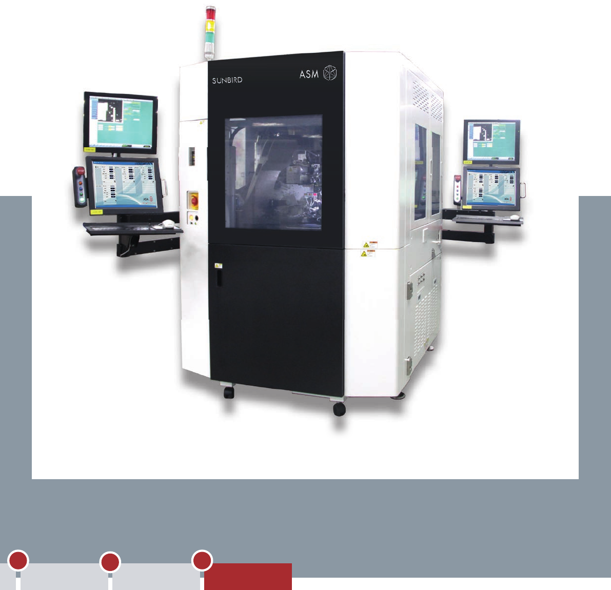
SUNBIRD
Extremely efficient inspection, sorting
and taping
▪ Combines various optical and electrical inspection
and (optional) laser marking capabilities in one
machine
▪ More reliable detection of faults by individual optical
inspection
▪ Maximum speed of 30,000 UPH thanks to turret
system
▪ Contactless alignment and smart chip handling
ensure optimal package protection
▪ Handling of smallest components (0603/0402 metric)
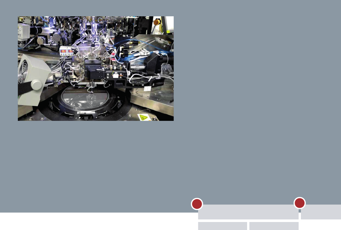
Dies are picked directly from the wafer to the turret system and transported
through various optical inspection and electrical test positions.
Six-side inspection, electrical tests,
laser marking, sorting and taping – the
SUNBIRD system combines a series of
functions in a single machine. And best of
all, thanks to the SUNBIRD turret system,
it does it all with a high degree of speed
and efciency.
In a rst step, the machine picks up the
packages with its ip arm, inspects their
bottom side and passes them to the turret,
where they are inspected from six angles,
tested, and optionally laser-marked.
Thanks to the SUNBIRD‘s smart iPrecise
and iAlign technologies, the alignment of
all components is ensured and optimized
via powerful optics and without any additi-
onal transfers.
Next, the SiP components are gently positi-
oned in tape pockets with automatic Z-axis
alignment, under the continuous check
of a vision system, which was especially
developed for this purpose. That way, even
extremely small, thin and sensitive dies can
be inspected and taped perfectly.
The nal sorting step: Divided by software
into separate classes, the machine places
the components into the tape or different
containers. With processing speeds of up
to 30,000 UPH, SUNBIRD represents a
signicant speed and quality improvement
over traditional systems.
WLP Inspection, Test & Packing
Finalizing your WLP/PLP processes:
SUNBIRD for inspecting, sorting and taping
16
Stencil Printing
Ball Drop Singulation
WLP Inspection,
Text & Packing
3
4
5
17
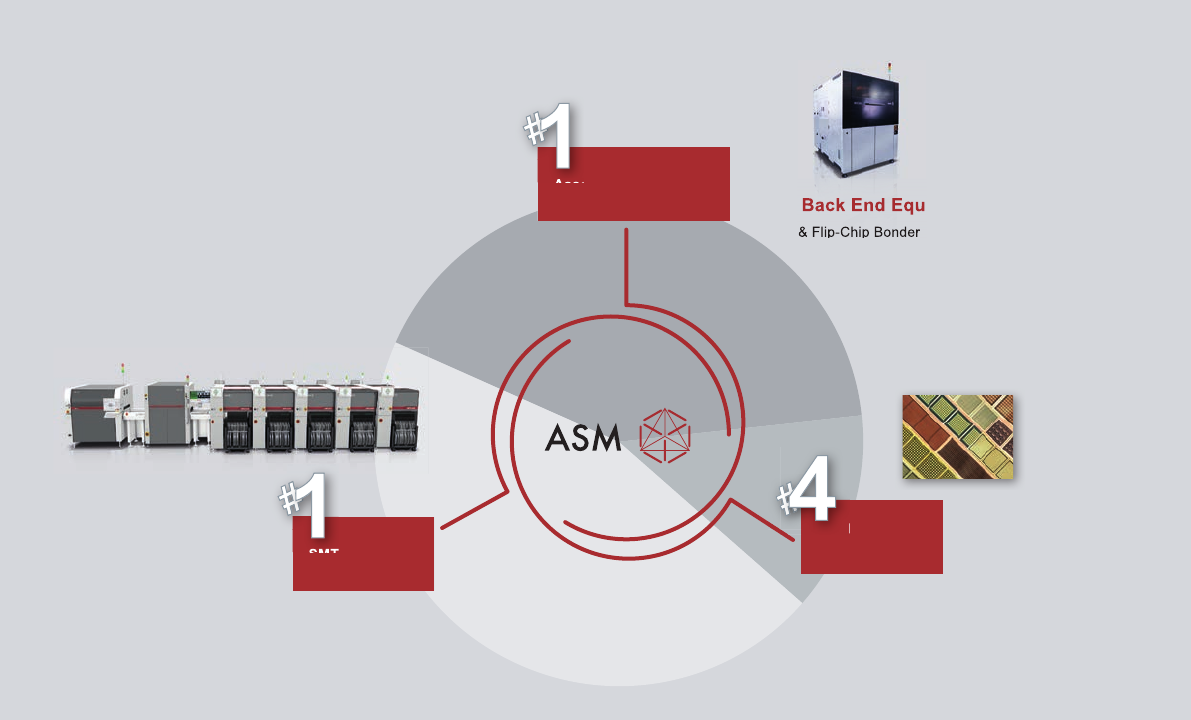
ASM SMT Solutions
▪ SMT Line Solution
▪ DEK Printing Solutions
▪ SIPLACE Placement Solutions
▪ ASM Smart Factory
Tools & Services
ASM Materials
▪ Leadframes
▪ Other Materials
▪ Molded Interconnect
Substrate (MIS)
ASM Back End Equipment
▪ Die & Flip-Chip Bonder
▪ Wire Bonder
▪ Encapsulation Equipment
▪ Tester & Sorter
▪ Laser Dicing
▪ LED Equipment
ASM Pacific Technologies
Market
SMT Equipment
(Printing & Placement)
SMT Equipment
Market
Assembly & Packaging
Equipment
Assembly & Packaging
Market
Leadframes
Market
ASM Back End Equipment
Die & Flip-Chip Bonder
The underlying idea makes a lot of sense.
Instead of combining the components for
a module on the circuit board, advanced
packaging rst integrates dies or ip-chips
with other SMT components into an SiP,
which is then placed on the board.
This process allows for further miniatu-
rization, eliminates the time-consuming
wire-bonding of dies and frees users from
designing required functionalities on their
own. The complete function group can be
placed as a single module.
This convergence of chip assembly and
SMT processes opens up new opportu-
nities. Whether semiconductor makers
or electronics manufacturers enter this
new market – either industry requires the
other’s process knowledge and expe-
rience.
ASM is your partner of choice
ASM is active in both segments. It is the
world’s only equipment supplier that has
been active and successful in both indus-
tries – chip assembly and SMT.
Invest in a growth market
Major trends like digitalization and networking are currently strengthening
the interest in advanced packaging technologies worldwide.
18