Brochure-PacTech-Electroless-Plating-Solder-Bumping.pdf
T ur nkey Solution for Electr oless Plating & Solder Bumping www .pactech.com
Turnkey Solution for
Electroless Plating & Solder Bumping
www.pactech.com
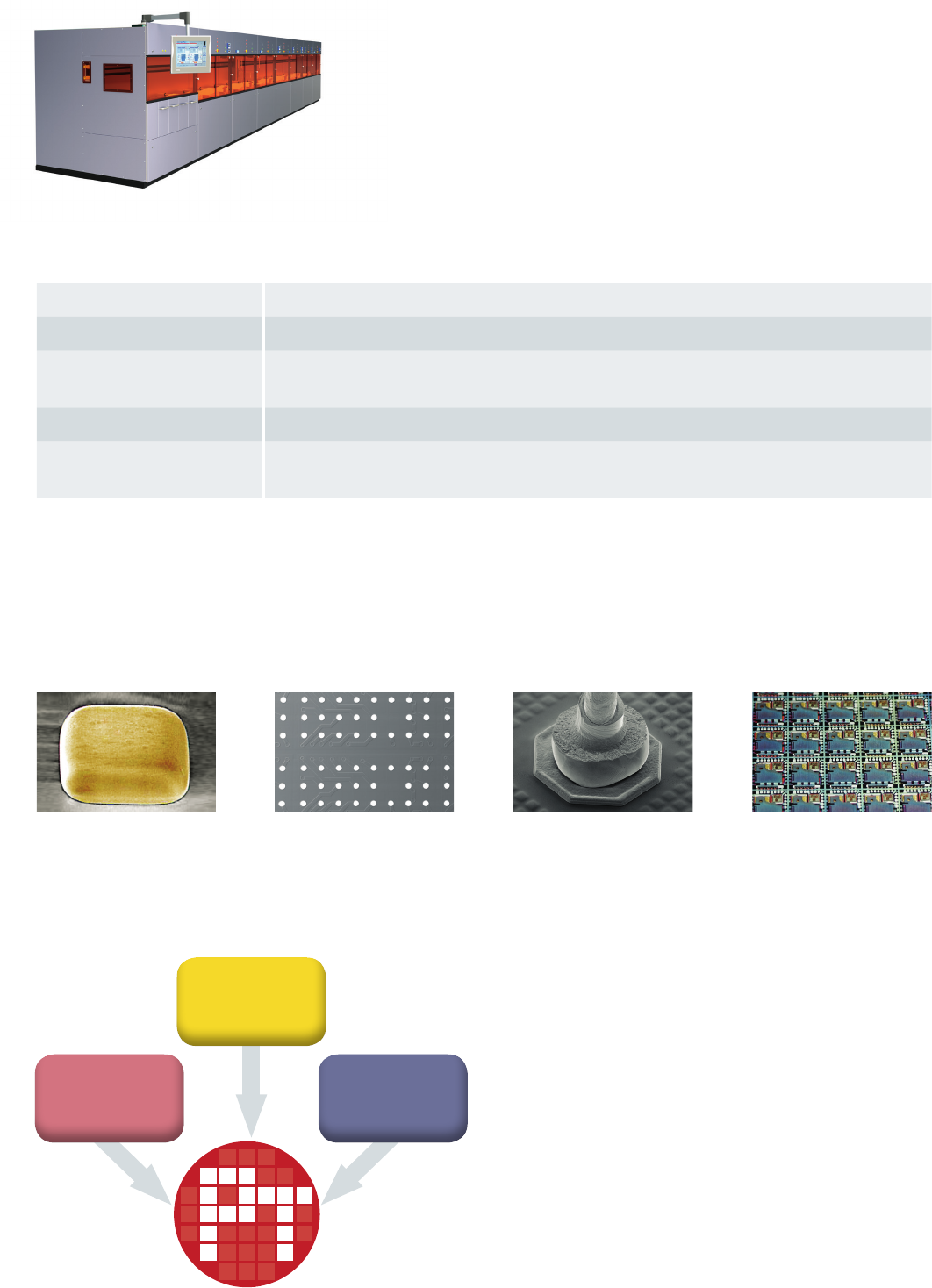
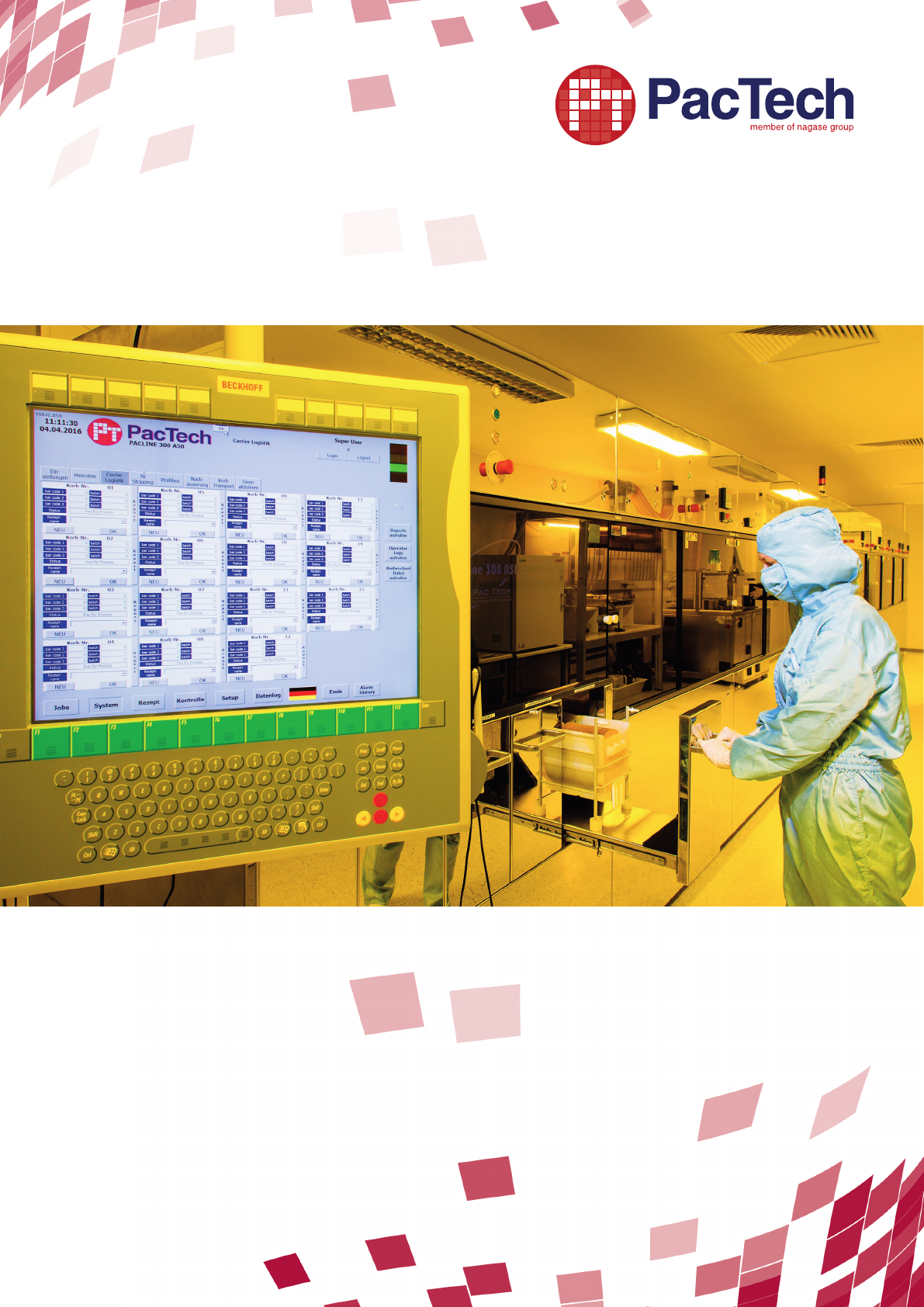
PacLine 300 – Electroless NiAu/NiPd/NiPdAu
RFID adhesive attach
on antenna
WLCSP, FlipChip
• Low cost, high reliability metal interface
• Mask-less process
• Fully automatic, dry-in dry-out
• In-linetemperature,pH,owcontrol
• Automatic chemical delivery and drain system
• SECS GEM interface
• CN / CN-free chemical options
Substrate Size
4” – 12” wafers, panels up to 650 mm x 650 mm
Substrate Thickness
≥100µm,thinwafersolutionavailableuponrequest
Substrate Materials
Si, GaAs, SiGe, InP, LiTaO3, Ceramics, Laminates, Glass, Quartz,
othermaterialsuponrequest
Pad Material
AlCu,AlSiCu,Cu,Al,AlSi,othermaterialsuponrequest
Machine Throughput
• UPH up to 150 wafers (8”)
• UPH up to 75 wafers (12” / Panel)
ProcessSpecications
Cu and high reliability Au
wirebonding
Clip attach
Major Applications
UniqueTurnkeySupplyandSupport
• Processexpertise,equipmentmanufacturingand
chemicals supply under one roof
• E-less plating solution tailored for all volume demand
• Worldwide second source support via PacTech’s
manufacturing sites in Europe, USA and Asia
• Development support in the time zone of
customer’s R&D center
• Turnkey process transfer to customer possible
at any time
Process
Equipment Chemicals
PacLine 300 – Electroless NiAu/NiPd/NiPdAu
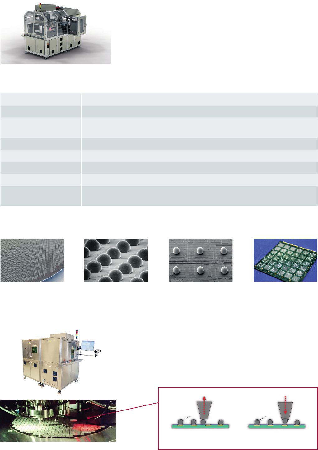
Ultra-SB
2
– Solder Ball Placement
• Optional FOUP wafer handling system
• Optionalprocessautomationwithintegrateduxing
• Optional pre and post placement stencil inspection
for better process control
• Optional integration of Ultra-SB
2
WLR for
automatic yield improvement
• Customizable in-line manufacturing adaptation
• Dedicatedequipmentsolutionforpanellevelisavailable
Substrate Size
4” – 12” wafers, panels up to 650 mm x 650 mm
Substrate Thickness
≥150µm,thinwafersolutionavailableuponrequest
Substrate Materials
Si, GaAs, SiGe, InP, LiTaO3, Ceramics, Laminates, Glass, Quartz,
othermaterialsuponrequest
UBM Material
AlCu,AlSiCu,Cu,Al,AlSi,othermaterialsuponrequest
Solder Alloy Material
SAC, AuSn, PbSn, SnBi, other Eutectic and high lead alloys
Ball Diameter
60µm–760µm
Ball Pitch
>100µm
Machine Throughput
• UPH≥40wafers(8”)
• UPH≥25wafers(12”)
ProcessSpecications
WLCSP FlipChip
Fan-in and Fan-out WLP
Bumping on Substrate
Major Applications
Ultra-SB
2
WLR – Wafer Level Rework
• Integrated 2D AOI
• Integrated rework capability for yield improvement
• Optional AOI map update capability
• Ballsizes:60µm–760µm
• UPH 8” ~25 wafer/hour
• UPH 12” ~15 wafer/hour
Repair bondhead
Removal of rejected solder ball Replacement of removed/
missing solder ball
Wafer
Solder Ball Capillary
Vacuum
Wafer
Solder Ball Capillary
Nitrogen