SJ401DCB1-05E_1.0.0_mail.pdf
Model 3Xi-M110 Resolution 10µm-30µm Target PCB Size mm (in.) 50W x 120L - 360W x 330L (1.97W x 4.73L - 14.17W x 12.99L) 50W x 120L - 360W x 510L ※ (1.97W x 4.72L - 14.17W x 20.07L)※ PCB Thickness 0.8mm - 4.0mm (0.031-0.1…
Model 3Xi-M110
Resolution 10µm-30µm
Target PCB Size
mm (in.)
50W x 120L - 360W x 330L
(1.97W x 4.73L - 14.17W x 12.99L)
50W x 120L - 360W x 510L ※
(1.97W x 4.72L - 14.17W x 20.07L)※
PCB Thickness 0.8mm - 4.0mm (0.031-0.157 in.)
PCB Warpage 2mm (0.08 in.) or less
PCB Clearance
TOP:60mm (2.36 in.)
Bottom:40mm (1.57 in.)
Inspection
Categories
Chip Type Parts, Diodes,
Tantalum Capacitors,
Aluminum Electrolytic Capacitors,
Module chips, Transistors,
Power Transistors, Connectors, QFP, SOP,
CSP, QFN, and BGA
Detector Flat Panel 14bit 3M Pixel
X-ray Tube 110kV 30W, Closed X-ray Source
X-ray leakage 0.5μSvh or less
Conveyor Method Flat belt transfer
Conveyor Height 880-920mm (34.65-36.22 in.)
Width Adjustment Auto Width Adjustment
Operating System
Windows 10 IoT Enterprise2019 EMB 64bit
(Microsoft)
Electric Power
Requirement
Three - Phase
~200 +/-10%, 50/60Hz
Power Consumption
4.2kVA
Air Requirement 0.5 MPa, 20 L/min(ANR)
Usage Environment 15°C - 30°C / 15 - 80%RH (Non-condensing)
Noise Level 70.0dB or less
Dimensions
W x D x H (Main body)
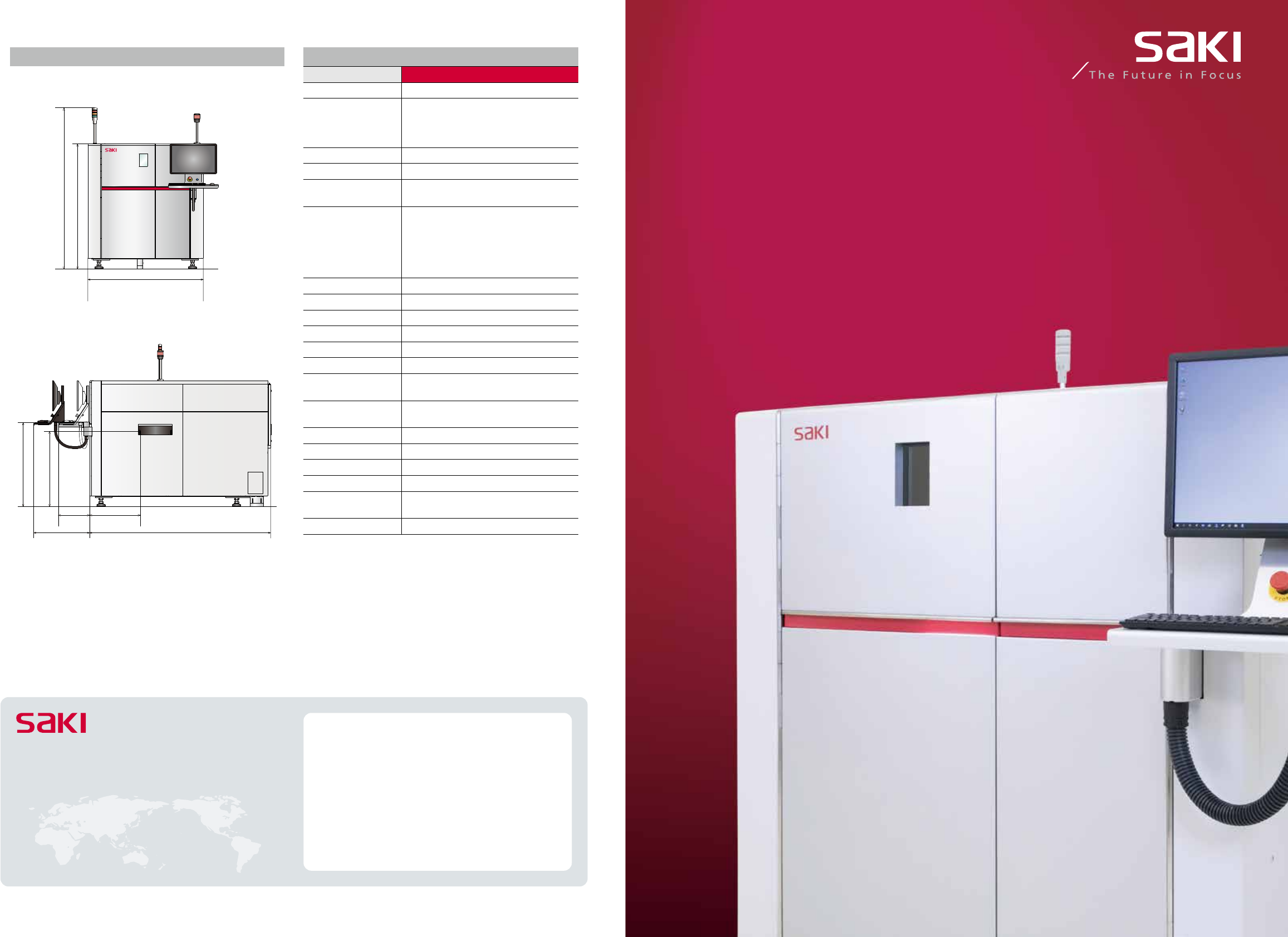
1380 × 2150 × 1500mm
(54.34 x 84.65 x 59.06 in.)
Weight (Main body) Aprox. 3,100 kg (6834.34 lbs)
Dimensions Hardware / Function Specications
■
Front View
Global Network
https://www.sakicorp.com/en/
Headquarters
DMG MORI Tokyo Digital Innovation Center
3-1-4, Edagawa, Koto-ku, Tokyo, 135-0051, Japan
TEL: +81-3-6632-7910 FAX: +81-3-6632-7915
Saki Corporation
© 2021 Saki Corporation. All Rights Reserved.
Specifications contained in this brochure are subject to change without notice.
This Brochure was made out in February 2021.
SJ401DCB1-05E
■
Side View
Inline 3D-CT Automated X-ray Inspection System
for Printed Circuit Board Assemblies (PCBAs).
3Xi-M110
1500 mm
1000 mm
900 mm
1940 mm
1380 mm
2150 mm(665 mm)
600mm
(370mm)
Side View
Front View
Top View
1500 mm
1000 mm
900 mm
1940 mm
1380 mm
2150 mm(665 mm)
600mm
(370mm)
Side View
Front View
Top View
※ with applying the two-step imaging option
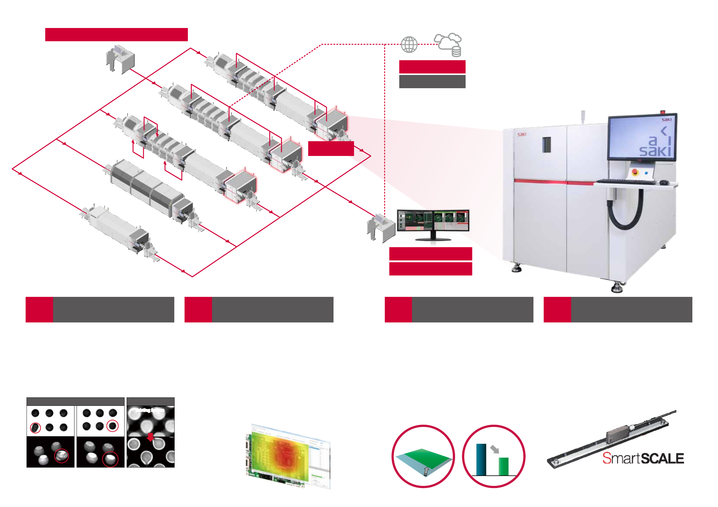
3D AXI
3D AOI
3D SPI
3D AOI
THD AOI
Feed Forward
Feed Back
Coating AOI
Saki Self-Programming & Self-Tuning
Judgement Station
Multi Process View
SPC & Report
MES & ERP
Internet
Cloud-based
Management System
2 3
The Ultimate
in Inspection Speed
and Accuracy.
• Revolutionary x-ray tube reduces x-ray exposure
up to 70% by powering on x-rays only at the mo-
ment of image capture
• Exposure dose simulator lets the user monitor the
radiation dose
• The method and magnification for releasing the
x-rays can be set
• Periodic maintenance and spare parts are not re-
quired
• Built-in monitoring system reports when the tube
needs replacing
• The 3Xi-M110 ensures hidden solder joint quali-
ty for bottom-electrode packages such as BGAs,
LGAs, and QFNs
• PCT provides precise volumetric measurements
and shape reconstruction to find voids, head-in-
pillow (HiP), and other defects that are extremely
difficult to identify
• 40% lighter hardware platform (3,100kg) and a
25% smaller footprint (1,380mm width)
• Saves floorspace, is easily installed, and improves
production-line operability
• Light, but rigid cast iron frame for stable opera-
tion and accuracy
• Optimized imaging range for PCBs up to 360 x
330mm (W x L)
• 2-step image capture is available for larger 360 x
510mm (W x L) boards
• Reliable and consistent positioning accuracy and
speed
• Double motor-driven system and high-precision
linear scale by Magnescale assures precision and
power
• Optimized Planar Computed Tomography (PCT)
technology algorithm improves image capture
speed by 30%, reducing takt time
Merit
3
Lightweight, rigid structure in
a small footprint
Merit
4
High accuracy and speed
Merit
2
Reduced x-ray exposure
Merit
1
Saki's planar CT technology
captures hard-to-find defects
About
30%
Weight saving
Weight
4.10m
2
2.97m
2
About
25%
Space saving
Footprint
Head in Pillow
Slice
Less Solders
Slice
Existing System
New AXI
NG Defective
Image Improvement