discoTR16-09_The effects of edge trimming_20160610.pdf
DISCO Technical Review Mar. 2016 1 The effects of edge trimming Engineering R&D Division, Operation V Abstract In recent years, the thickness of flash m emory and its controller chips has been re duced due to the min…
DISCO Technical Review Mar. 2016
1
The effects of edge trimming
Engineering R&D Division, Operation V
Abstract
In recent years, the thickness of flash memory and its controller chips has been reduced due to the
miniaturization and the capacity enlargement of smartphones and tablet devices. Moreover the
requirements of more precision thinning process and yield improvement become more severe in
manufacturing process. An edge chipping at the outer area of the wafer, which causes wafer breaking, is
one of critical issues in ultra-thinning process due to the influence of rounded shape. A process called
“Edge trimming” effectively removes the rounded shape on the outer edge of the wafer which causes
edge chipping, preventing the wafer from breaking. In this review, we report the effects of edge trimming,
which has been adopted for improving yield when performing ultra-thin wafer grinding.
1. Introduction
During wafer ultra-thinning, the edges chipping
because of the rounded shape of the wafer's outer
edges induces wafer breaking. Therefore, a
process called "edge trimming" is employed to
remove the rounded area at the outer edges using
a blade before grinding.
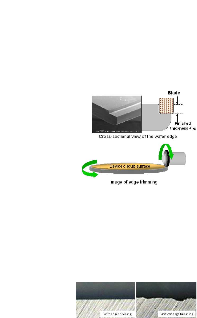
There are the two edge trimming methods: edge
trimming before bonding, in which the device
wafers are processed from the front before
bonding, and edge trimming after bonding, in
which the device wafers are fully cut from the
back after carrier wafer bonding.
For the edge trimming before bonding, depth of
approximately 150-200 µm is cut from the surface
of the device wafers. Thus, this method is better
than the edge trimming after bonding in terms of
edge-chipping size and feed speed. However, as
the surface of the device wafer is exposed, it
might cause particle contamination and contact on
the device surface during wafer handling (Fig. 1).
In contrast, for the edge trimming after bonding,
the device wafers must be fully cut, and the
cutting amount almost equals to the original
thickness of the silicon (Si) wafers. Thus, higher
cutting capability is required for the blade than
that required in edge trimming before bonding.
Therefore, a blade with larger grit size is normally
used. The feed speed is usually set at low
considering the processing load. However, as the
wafers are already bonded, particle contamination
and contact on the device surface during wafer
handling are prevented.
This review presents the test results to verify the
effect of edge trimming before bonding in the
wafer grinding process.
2. Effect of edge trimming and process
verification
2.1 Effect of edge trimming
To verify the actual effect of edge trimming,
wafers with and without trimmed edges were
ground and their chipping at the edge sections
were compared.
The results in Fig. 2 show that grinding without
edge trimming caused edge chipping; however,
grinding with edge trimming allowed mitigating
this problem.
Fig. 2 Wafer edges after grinding with and without
edge trimming
Fig. 1 Edge trimming
DISCO Technical Review Mar. 2016
2
2.2 Process verification
For processing, a dicing saw with blades of
thickness 1-3 mm was used. The width for edge
trimming is generally 0.5-3 mm, and the blade
thickness is determined depending on the process.
After the edge is trimmed using the blade, the
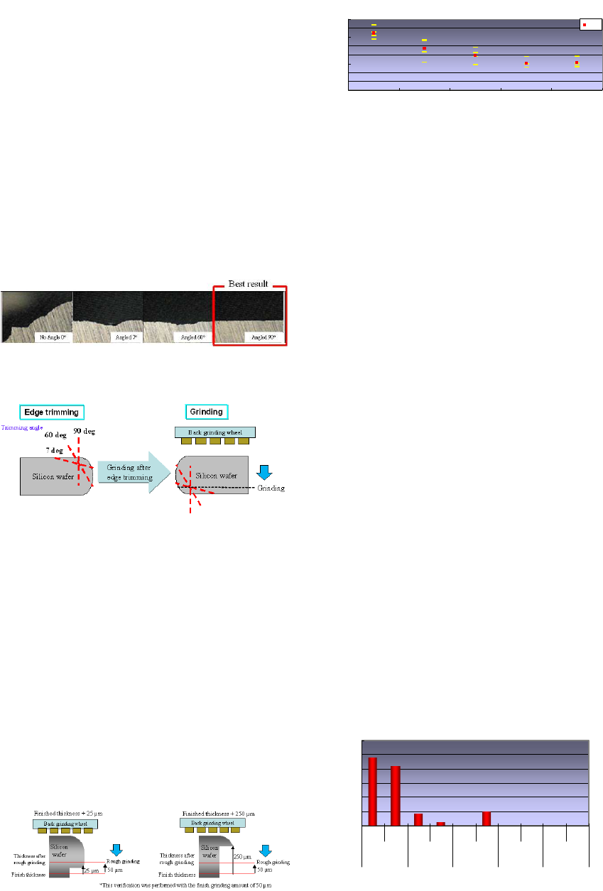
edge shape normally has an angle of 90°. To
determine the most effective trimming angle, the
angles were compared. Fig. 3 shows the images of
the compared angles. This confirms that edge
trimming is most effective for reducing edge
chipping when the angle is 90°. At other angles,
edge chipping occurs because the effect of edge
trimming is insufficient. Fig. 4 shows the
verification process with various edge trimming
angles.
Fig. 3 Comparison of edge trimming angles.
Fig. 4 Process of this verification with various edge
trimming angles
Next, the adequate depth of edge trimming was
verified. Thinning after edge trimming is usually
conducted in two stages of rough and fine
grinding. After edge trimming, the remnant part is
removed during a low-speed process of the rough
grinding (Fig. 5). Based on the assumption that
the depth of the damage created during this
process may relate to edge chipping, the extent of
the damage after rough grinding was examined.
Fig. 6 shows the extent of damage at each cutting
depth of edge trimming. This graph confirms that
the remnant section was removed when it was
thinned through rough grinding, and the wafer
was damaged.
Fig. 5 Grinding in this review
Damage depth at the edge section after rough grinding
0
10
20
30
40
50
60
70
80
Finished thickness
+ 25 µm
Finished thickness
+ 60 µm
Finished thickness
+ 80 µm
Finished thickness
+ 100 µm
Finished thickness
+ 250 µm
Edge trimming cut depth (µm)
Damage depth (µm)
Avg
*Varies depending on the processing parameters.
Fig. 6 Damage depth in the Z-direction after rough
grinding.
The wafers were thinned and polished to their
finished thicknesses to verify edge chipping. Fig.
7 shows the number of edge chippings. This graph
confirms the correlation between the number of
edge chippings and the extent of damage due to
rough grinding. When the edge is trimmed for a
finished thickness plus 100 µm or more, edge
chipping can be prevented.
The aforementioned results show that a finished
thickness plus 100 µm is recommended as the
adequate edge trimming depth based on the
assumption that the fine grinding depth is 40 µm.
The recommended width of edge trimming differs
depending on the bonding method. Chemical
mechanical polishing (CMP) is normally
performed when fabricating interconnects on
wafers. Owing to the characteristics of CMP
process, the outer edges tend to be lower than
center area. The lower areas vary depending on
the process and are usually below 3 mm from
the outer edges. Therefore, when the wafers are
bonded through oxide bonding, which is used in
the manufacturing of Backside Illumination
CMOS sensors (BSI; a type of image sensor), it
produces areas at the outer edges of a wafer where
bonding is insufficient. If these wafers are ground,
it may cause problems, such as peeling. Thus, the
recommended edge trimming width is 3 mm. In
resin bonding, which is used in the manufacturing
of 3D-IC using through-silicon vias (TSVs), gaps
0
5
10
15
20
25
30
1st 2n d 1st 2n d 1st 2n d 1st 2nd 1st 2nd
Finished th ickness
+ 25 µm
Finished th ickn ess
+ 60 µm
Finished th ickness
+ 80 µm
Finished th ickness
+ 10 0 µm
Finished th ickn ess
+ 25 0 µm
Numb er of edge chipp ings
Fig.7 Comparison of the number of edge chippings
DISCO Technical Review Mar. 2016
3
caused by the lower areas at the outer edges can
be absorbed by the resin thickness. Thus, no
insufficient bonding areas are produced.
Therefore, the edge-trimming width must be
considered only at the rounded areas of wafer
edges. The width of the rounded area is often
approximately 0.3-0.4 mm. It is necessary to
completely remove this area, and thus the
recommended width is 0.5 mm, considering the
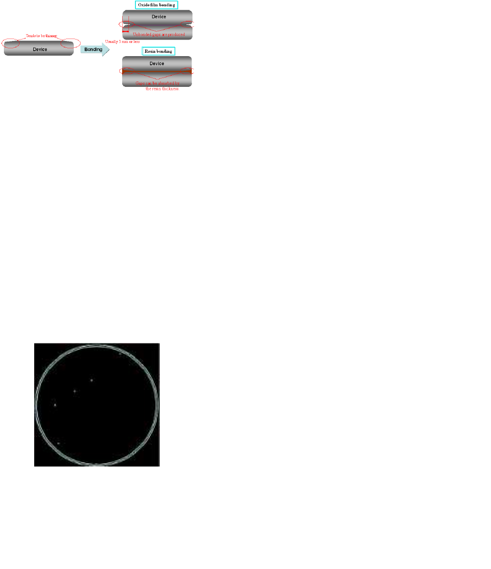
processing variation. Fig. 8 shows edge
conditions after each type of bonding.
3. Introduction of edge trimming in FEOL
(Front-End-of-Line) processes
Edge trimming before bonding requires high-level
cleanliness because the device wafer must be
bonded to a carrier wafer in the subsequent
process. Therefore, we developed the advanced
equipment that can handle the edge clamp transfer
system and chemical cleaning. Fig. 9 displays a
particle counts after edge trimming using the
advanced equipment. The result shows five
particles with sizes of 0.1 µm or less (edge
exclusion: 4 mm).
Edge trimming has gradually been adopted in
FEOL processes. We will further evaluate and
develop this technology to satisfy the requirement
in the advanced device process.
4. Conclusion
As explained in this review, edge trimming is
essential to meet the ultra-thinning process of Si
wafers. We have verified and evaluated this
technology to achieve the best results. In the
future, to provide optimal applications with
enhanced performance, we will verify edge
trimming for materials currently available but not
limited to Si wafers.
Fig. 9 Particle map
Fig. 8 Edge conditions after bonding
Inquiries of "DISCO Technical Review"
Sales Egnineering dept., DISCO CORPORATION
Phone:+81
-
3
-
4590
-
1115