SM-131-006.pdf - 第221页
Device Name Chip Mounter Block Name Page No. Unit Name Revision Model Item GXH-1 Chapter 13 Layout of Electrical 1. Layout of Underframe Layout 1.3 Layout of BH Blocks Symbol Name G01 DC Power Unit (For Safety Circuits, …
Device
Name
Chip Mounter
Block Name
Page No.
Unit Name
Revision
Model ItemGXH-1
Chapter 13 Layout of Electrical
1. Layout of Underframe
Layout
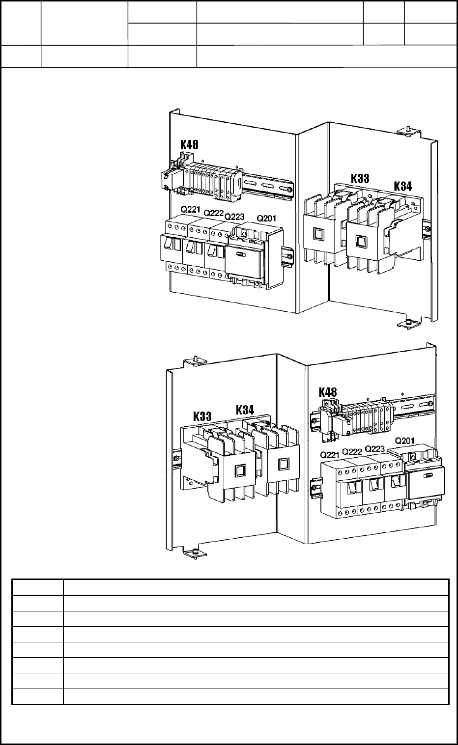
1.2 Layout of BG Blocks
Fig. M5
Section A on L Side
Section D on R Side
Fig. M6
Section B on L Side
Section C on R Side
Symbol Name
Q201 Secondary Power Breaker (Power Supply to Beams)
Q221 Breaker (X-Axis Power Supply)
Q222 Breaker (Y1-Axis Power Supply)
Q223 Breaker (Y2-Axis Power Supply)
K33 Magnet Contact Switch (For Beam)
K34 Magnet Contact Switch (For Beam)
K48 Relay (For Beam)
0406-001
13-3
Device
Name
Chip Mounter
Block Name
Page No.
Unit Name
Revision
Model ItemGXH-1
Chapter 13 Layout of Electrical
1. Layout of Underframe
Layout
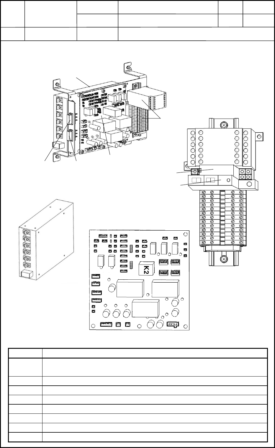
1.3 Layout of BH Blocks
Symbol Name
G01 DC Power Unit (For Safety Circuits, Externals via I/O and I/F, Head Multiaxis,
Controls, etc.)
U26 Relay Board 1 (UB20)
F011 Fuse (For Power Supply to Externals via I/F of Input and Output Machines)
F031 Fuse (For Cooling Fan on Left Side of Machine)
F032 Fuse (For Cooling Fan on Right Side of Machine)
K2 Power ON Delay Timer
K3 Relay
K51 Relay (Fan Power Supply)
G01
A
U26
F031
F032
Fig. M7 Whole View of BH Block
K3
K51
F011
Fig. M8 Section A
G01
Fig. M9 G01 Section
Fig. M10 U26
0406-001
13-4
Device
Name
Chip Mounter
Block Name
Page No.
Unit Name
Revision
Model ItemGXH-1
Chapter 13 Layout of Electrical
1. Layout of Underframe
Layout
1.4 Layout of BA and BC Blocks
0406-001
13-5
A63 in Section A
A63 in Section B
A53
K49
K50
K40
K39
K60
K72
K71
K75
K76
K77
K78
(F021B to F024B)
(
F021A to F024A
)
R01A and R01B
behind Panel
Fig. M11 BA Block
A63 in Section D
A63 in Section C
A53
(F033~F036)
(F021D~F024D)
(F021C~F024C)
K75
K76
K77 K78
R01C and R01D
behind Panel
K40
K39
K49
K50
K60
K72
K71
Fig. M12 BC Block