KY8030 Programmers Manual.pdf - 第63页
Program mers Manual | 6 1 ● Trace It is a defined straig ht line data which is included in the St encil and Mask plane of the Gerber file. It is a data that is required to process a Board by moving along the straight lin…

60 | KY-8030 Series(KYOS-2007001_rev0)
3DIn‐lineSolderPasteInspectionSystems
● GerbPad file
file used at GerbPad program to convert Gerb file (*.gbr) to pad file (*.pad).
● Pad file
It is a file that includes Pad data.
Format: There are various formats that can be chosen depending on a text file and
demand by a user.
① Position: X, Y, angle
② Size: Width, Length
③ Shape : Rectangle, Circle, Rounded rectangle, Oblong, P(Positive Sloped
Rectangle), N(Negative Sloped Rectangle), Undefined
● Job file
It is a file in which work data are saved.
Format: *.gpd
● Aperture file
It includes a defined straight line, a graphic shape and size data. There is a standard
format (GAP), however, a different format is used for each CAD software which
creates the Gerber file. It is loaded separately only for the RS-274D format.
● Stencil file
It is a Gerber file designed to produce stencils for screen printer. It is a SMD type
Pad data.
It is generally created in the Mask file.
● Mask file
It is a Gerber file used for Mask plane of the PCB. It is a SMD type and Hole type
Pad data.
The edited file after removing a Hole Pad from the Mask file is a Stencil file.
● Silk file
It is a Gerber file used for Silk plane of the PCB. It contains data of the reference and
auxiliary line.
● Flash
It is a template or window data which is included in the Stencil or Mask plane of the
Gerber file. It is a data that is required for processing the PCB with optic Flash after
putting a straight-sided or circular template(or window).
Programmers Manual
| 61
● Trace
It is a defined straight line data which is included in the Stencil and Mask plane of the
Gerber file. It is a data that is required to process a Board by moving along the
straight line with a straight-sided or circular tool.
● Pad
It is a part of the PCB. It is the part which is soldered and applied with lead. There
are 2 types of Pads. One is the SMD type Pad in which the SMD type parts are put,
and the other is the Hole type Pad in which Through-Hole type parts are inserted.
● Pattern
It is a group of the Flash and Trace which are connected with each other and their
shapes, sizes and angles are same. All the Pads, letters and symbols that exist on
the Mask (Stencil) are patterns. Generally a group of many Pads is used as a Pattern.
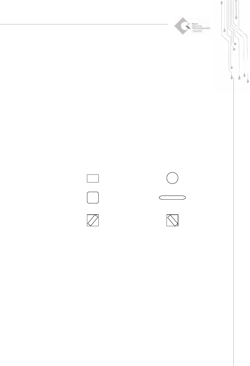
● Shape
It is a shape data which is used for Patterns, Pads and Apertures.
Example)
rectangle (Rectangle) Circle (Circle)
Rounded Rectangle (Rounded Rectangle) Oblong (Oblong)
P-type (Positive Sloped Rect.) N-type (Negative Sloped Rect.)
Other (Undefined)
● Reference
It is a name of the components. It is used for distinguishing the positions of the
components on the PCB.
● Pattern data
It is a Pattern information.
Shapes, X axis position, Y axis position, reference
62 | KY-8030 Series(KYOS-2007001_rev0)
3DIn‐lineSolderPasteInspectionSystems
1.5. PAD File specifications
● Specifications
@HEADER
Version= <nVersionNo>
Unit=<szUnit>
Coordinate=<szCoordinate>
OffsetX=<fOffsetX>
OffsetY=<fOffsetY>
Arrays=<nArrays>
Fiducials=<nFiducials>
CheckPoints=<nCheckPoints>
Patterns=<nPatterns>
Pads=<nPads>
@BOARD
<fBoardSizeX> <fBoardSizeY>
@ARRAY
<nArrayNo> <fShiftX> <fShiftY> < fShiftR>
@FIDUCIAL
<nFidNo> <cFidType> <cFidShape> <fFidX> <fFidY> <fFidSizeX> <fFidSizeY> <fFidOffsetX>
<fFidOffsetY> <dbsRefCode>
@CHECKPOINT
<nCheckPointNo> <fCheckPointX> <fCheckPointY>
@PATTERN
<nPatternNo> <cShape> <fPatternSizeX> <fPatternSizeY> <fPatternOffsetX> <fPatternOffsetY>
<fPatternArea> <fPatternAngle>
@PAD
<nPadNo> <nPatternNo> <fPadX> <fPadY> <dbsRefCode>
@END