F5HM Circuit Diagrams.pdf - 第72页
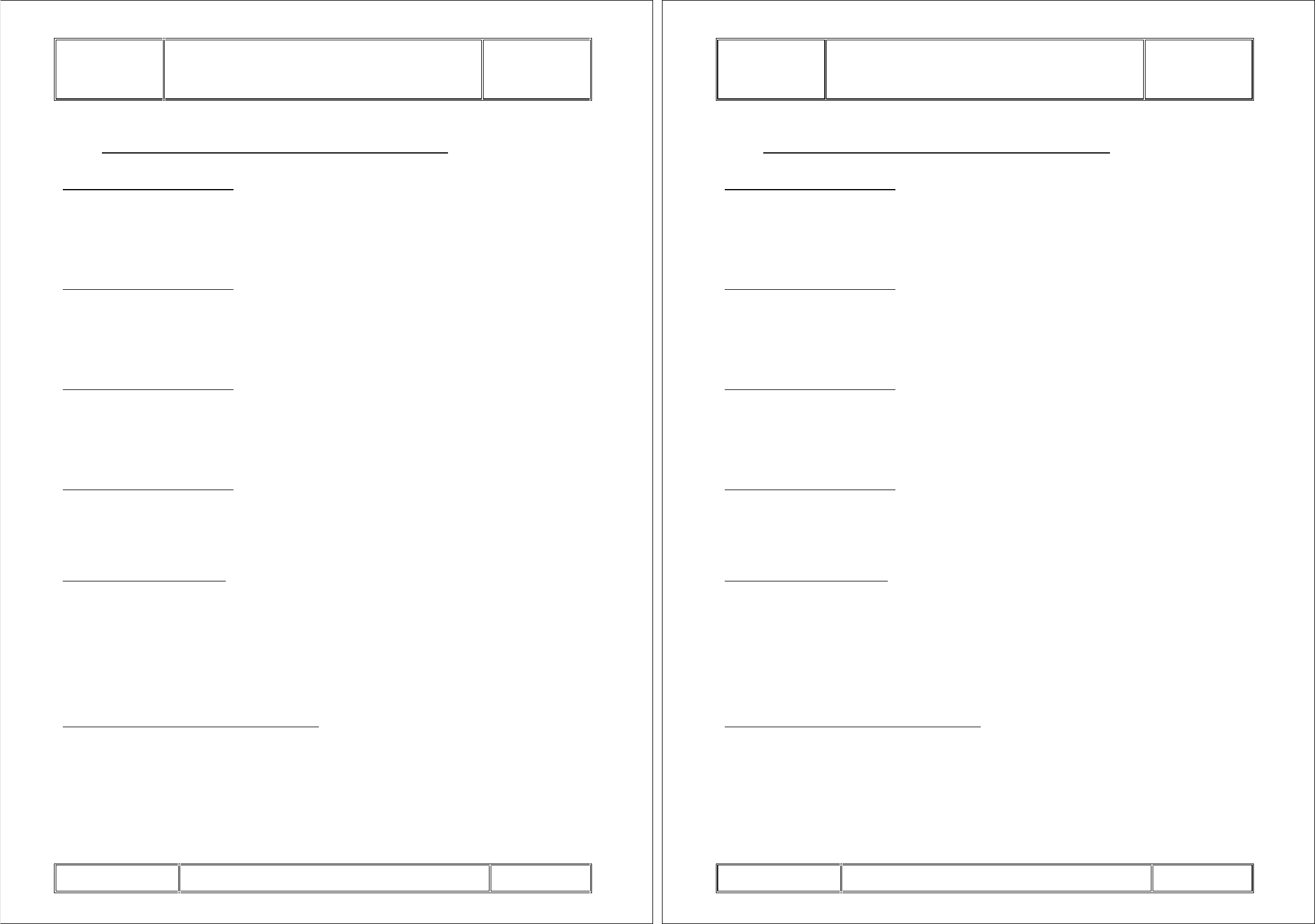
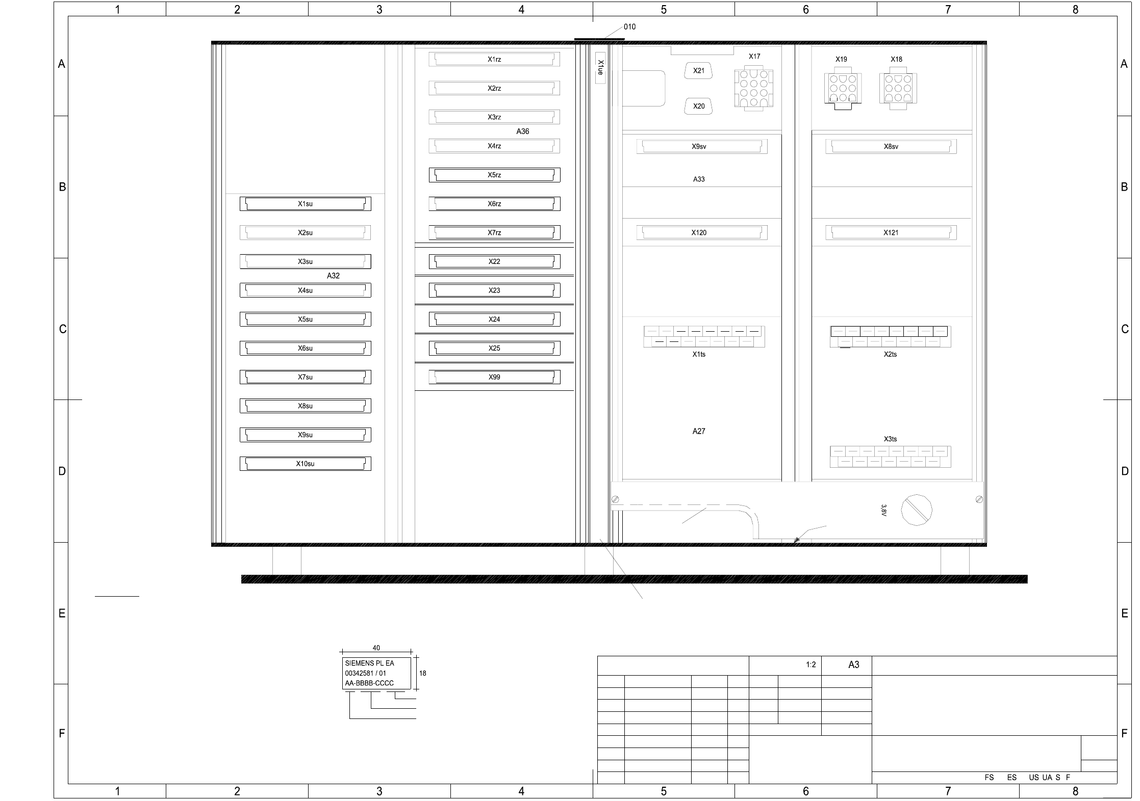
2 Circuit Diagr ams 72 0034258 1-040101 FD4 F5 HM con trol unit , base (wra p connectio ns) (Sh. 3 of 3) 6LHPHQV$* :UDSFRQQHFWLRQV 'UDZLQJQXPEHU )' 'HVLJQDWLRQ 6+0FRQWUROXQLWED…
2 Circuit Diagrams 71
00342581-040101FD4 F5 HM control unit, base (wrap connections) (Sh. 1 of 3)
00342581-040101FD4 F5 HM control unit, base (wrap connections) (Sh. 2 of 3)
6LHPHQV$*
:UDSFRQQHFWLRQV
'UDZLQJQXPEHU )'
'HVLJQDWLRQ 6+0FRQWUROXQLWEDVH
3/($(
5HVSRQVLEOH3/($(5HI
:ROOJDUWHQ
6LJQDWXUH 7HVWGHSDUWPHQW 'HYHORSPHQWGHSDUWPHQW 3DJH RI
'DWH
S23 Control Unit, Wrap connections incl. M54
(AMS bus with 7 slots)
Coding, axis board 1 (SP3):
Axis no. 0 (module 1)
Axis no. 1 (module 2)
Axis no. 2 (module 3)
SMP-SP3 connection:
B7
⇔
B16
⇔
B19
Coding, axis board 2 (SP4):
Axis no. 3 (module 1)
Axis no. 4 (module 2)
Axis no. 5 (module 3)
SMP-SP4 connection :
B3
⇔
B4
⇔
B9
⇔
B16
⇔
B18
⇔
B20
Coding, axis board 3 (SP5):
Axis no. 6 (module 1)
Axis no. 7 (module 2)
Axis no. 8 (module 3)
SMP-SP5 connection :
B4
⇔
B5
⇔
B7
⇔
B8
⇔
B9
⇔
B16
⇔
B21
Coding, axis board 4 (SP6):
Axis no. 9 (module 1)
Axis no. 10 (module 2)
Axis no. 11 (module 3)
SMP-SP6 connection :
B3
⇔
B6
⇔
B8
⇔
B10
⇔
B16
⇔
B18
⇔
B19
⇔
B21
AMS interrupt axis boards
Connections:
AMS-SP6 / C7
⇔
SMP-SP3 / C15
⇔
SMP-SP3 / C17
⇔
SMP-SP3 / C19
⇔
⇔
SMP-
SP4 / C15
⇔
SMP-SP4 / C17
⇔
SMP-SP4 / C19
(AMS_INT2)
AMS-SP6 / A8
⇔
SMP-SP5 / C15
⇔
SMP-SP5 / C17
⇔
SMP-SP5 / C19
⇔
⇔
SMP-SP6 / C15
⇔
SMP-SP6 / C17
⇔
SMP-SP6 / C19
(AMS_INT3)
Coding for I/O boards 1 - 3 (SP8 - SP10):
Connections:
I/O board 1 SMP-SP8 / C31
⇔
SMP-SP8 / C23
⇔
⇔
SMP-SP8 / C25
⇔
SMP-SP8 / C27
I/O board 2 SMP-SP9 / C31
⇔
SMP-SP9 / C23
⇔
⇔
SMP-SP9 / C25
I/O board 3 SMP-SP10 / C31
⇔
SMP-SP10 / C23
⇔
⇔
SMP-SP10 / C27
2 Circuit Diagrams 72
00342581-040101FD4 F5 HM control unit, base (wrap connections) (Sh. 3 of 3)
6LHPHQV$*
:UDSFRQQHFWLRQV
'UDZLQJQXPEHU )'
'HVLJQDWLRQ 6+0FRQWUROXQLWEDVH
3/($(
5HVSRQVLEOH3/($(5HI
:ROOJDUWHQ
6LJQDWXUH 7HVWGHSDUWPHQW 'HYHORSPHQWGHSDUWPHQW 3DJH RI
'DWH
Connection between communications assemblies and ICOS:
Flat ribbon cable, 20-pin
Communications assembly for rear panel X99 Kombgr Rückwand X99 (via SP7)
ba
1
ul
Pin 1 on b1
2
ll
3
ll
4
ll
5
ll
6
ll
7
ll
8
ll
9
ll
10
l
✕
a10 is Key
11
✕✕
Pins cut out
MM
ICOS1 rear panel
X10sv
2 Circuit Diagrams 73
00342581-010102TD3 F5HM control unit, base (viewed from the front) (Sh. 1 of 2)
Stay bar
Fan unit A35 (ue)
* Note
Apply the following labels inside (flush with the front plate):
A: Identification label Assembly inscription acc. to VA-F-510-001
Font size 2.5mm, material: Scotchal 3698-E (color: AI RAL 9006)
B: Inspection label Identification: Testing engineer, month, year
Series number
Date (year/month/day) acc. to SN 01007
Manufacturer/location acc. to SN 37040
* Note
SMP bus board
AMS bus board
SV backplane
MVS backplane
Edge protection
Battery
(viewed from the front)
Massstab
02.
02.11.1998 Tekin
26.05.99
26.05.99
26.05.99
Tek
Tek
Tek
01.
01.
S23 control unit, basic module
00342581-020102TD3
Copying of this document, and giving it to others and the use
or communication of the contents thereof, are forbidden with-
out express authority. Offenders are liable to the payment of
damages. All rights are reserved in the event of the grant of
a patent or the registration of a utility model or design.
Blatt
Bl.
(Zeichnungsnummer)
Norm
Gepr.
Bearb.
Datum
Name
NameDatumMitteilungZustand
PL EA 1 E2
SIEMENS
Stamm-Nr.
1
2
SMD-Placement System Siplace S23
Product status
Doc. status
Function status
Schadenersatz. Alle Rechte fuer den Fall der Patenterteilung
ausdruecklich zugestanden. Zuwiderhandlungen verpflichten zu
Weitergabe sowie Vervielfaeltigung dieser Unterlage, Verwer-
oder GM-Eintragung vorbehalten.
tung und Mitteilung ihres Inhalts nicht gestattet, soweit nicht
26.05.99