NordsonDAGE-SMTAI-2014.pdf - 第4页
Figure 3. Example of a ductile or so lder failure due to shear test. The dark area in the middle is an interfacial void. The other type of failure o bserved during the shear tes t ing was a pad crater . This type of fail…
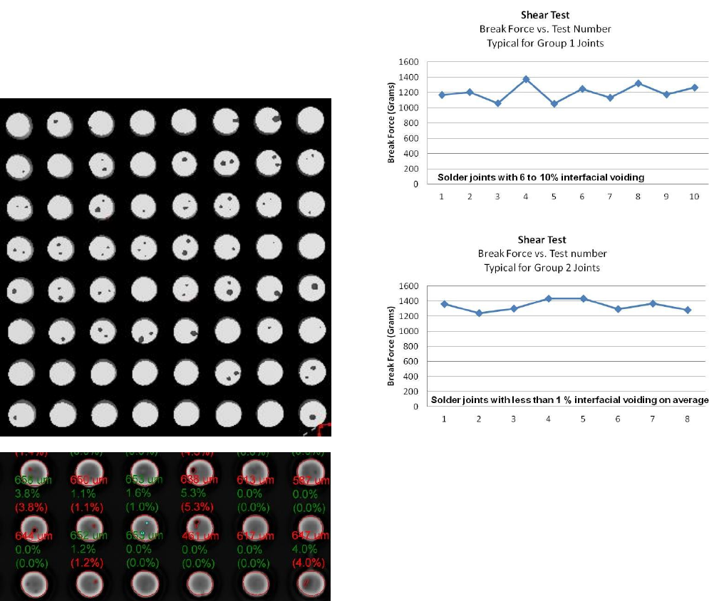
carefully scanned the device in question using Large Board
CT in order to produce a detailed map of the interfacial
voiding percentage at the PCB interface. Once done, we
started polishing down the device in order to reveal the
solder joints and prepare for the shear testing. This process
needs to be carried out very slowly and carefully in order
not to disturb the joint’s integrity. Before proceeding with
the shear testing, we grouped the pins in two groups: Group
1 - pins that exhibited 6% to 10% interfacial voiding and
Group 2 - pins with up to 1% on average interfacial voiding.
In order to do this we used electronic cross section data as
obtained by Large Board CT. Figure 1 shows a typical
electronic cross section or e-section of the interfacial area of
a BGA device. On Figure 1a the voids appear as the black
oval areas within the joint represented in white. On Figure
1b we show a typical voiding calculation carried on an e-
section at the interfacial area of the BGA device.
(a)
(b)
Figure 1. Electronic cross sections (e-sections) of interfacial
area of a BGA device. Black oval areas represent the
voiding (a), (b) BGA voiding calculation on an e-section at
the PCB interfacial area. These sections are obtained in a
completely non destructive way.
The shearing of the bonds was performed using a standard
Dage 4000 Plus bondtester. Contemporary bondtesters are
very versatile and accurate machines that perform a very
wide variety of mechanical tests both in a destructive and
non-destructive way. These include shear, pull, peel, and
also a large set of material tests like 3 and 4 point bend tests.
For certain testing conditions these machines can be
automated in order to achieve speed, productivity or better
accuracy.
Typical shear test results are shown on Figure 2. It is
obvious the joints in Group 2 (less than 1% interfacial
voiding on average) show more consistent and higher results
for break force compared to the joints in Group 1 (6% to
10% interfacial voiding).
(a)
(b)
Figure 2. Typical shear results for Groups 1 and 2 solder
joints. Group 2 joints (less than 1% voiding) show better
joint strength.
We observed two types of failure mechanisms due to the
shear testing – ductile and pad cratering, with the ductile
failure being significantly more proliferated. A ductile
failure is shown on Figure 3 and corresponds to a failure
that occurs in the solder bulk.
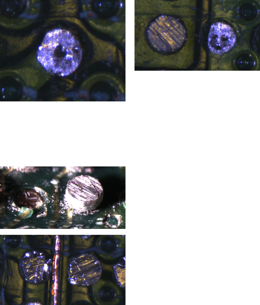
Figure 3. Example of a ductile or solder failure due to shear
test. The dark area in the middle is an interfacial void.
The other type of failure observed during the shear testing
was a pad crater. This type of failure is shown on Figure 4
and – the break occurs in the PCB material and it looks like
a crater.
(a)
(b)
Figure 4 – Pad crater failure due to shear test. The break
occurs in the PCB material; (a) side view, (b) top view
A comparison between pad crater and a ductile failure is
shown on figure 5.
Figure 5 – Comparison between pad crater (left) and ductile
failure (right). Interfacial voiding seen in the solder
After completing the shear testing, we averaged the results
and found the average value for break force for Group 1
joints (interfacial voiding 6% to 10%) to be 1192 grams. For
this study we considered only data points that represented
solder failure. The corresponding result for Group 2 joints
(less than 1 % voiding on average) was 1317 grams. This
indicates that he joints of Group 2 showed 9% to 10%
higher values for break force on average. This result is in a
good agreement with the hypothesis that interfacial voiding
affects negatively the bond strength. The device we used
for testing exhibited moderate levels of interfacial voiding
and we were still able to observe a negative impact on
solder strength. It was also very interesting to observe that
the weakest link for this device were pad crater failures that
occur around 800 grams shear force.
CONCLUSIONS
In this paper, we describe a testing procedure that combines
non destructive X-ray examination combined with
destructive shear testing in order to study the impact of
interfacial voiding on joint strength of BGA devices. We
used a X-ray Large board CT technique that permits a
virtual e-section to be taken at the BGA to PCB interface
and revealed the interfacial voiding. Previous study [1] has
indicated that the correlation between interfacial voiding
and total voiding as per IPC-610 can be very weak for
certain devices. Thus, being able to quantify the exact
amount of interfacial voiding is crucially important and can
be carried out only by employing Large Board CT. The
shear experiments were executed using a multi-purpose
Bondtester system that is capable of doing a large variety of
Bondtest experiments as well as many material tests like 3-4
bend test.
We found that interfacial voiding negatively impacts joint
strength up to 10% for a very moderate amount of
interfacial voiding (6% to 10%). We expect higher levels of
voiding to produce much stronger negative effect.
As a future work project we plan to expand our testing to
include a larger number and different types of BGA devices
in order to gain statistical significance and a better accuracy.
We hope to be able to study the effect of higher level of
interface voiding (15% and more), as we speculate that the
impact on the joint integrity would be more significant and
therefore critical.
ACKNOWLEDGEMENTS
The authors would like to thank Mr. Vineeth Bastin for
great help with this paper.
REFERENCES
[1] Evstatin Krastev and John Tingay, Recent Advances In
The X-Ray Inspection Technology With Emphasis On
Large Board Computer Tomography And Automation,
PanPac Microelectronics Symposium 2014
[2] Evstatin Krastev, D. Bernard, Dragos Golubovic , 3D
Board level X-ray inspection via limited angle computer
tomography’, , SMTAI, 2012
[3] Reference 3: S. Sethuraman et al., The Effect of Process
Voiding on BGA Solder Joint Fatigue Life Measured in
Accelerated Thermal Cycling, SMTAI conf. (2007).
[4] D.Hillman et al., The Last Will and Testament of the
BGA Void, SMTAI conf. (2011).
[5] G. Qin et al. Assessing the Impact of Temperature
Cycling Reliability of High Levels of Voiding in BGA
Solder Joints, SMTAI conf. (2012).
[6] ‘Modern 2d / 3d X-ray Inspection - Emphasis on BGA,
QFN, 3d Packages, and Counterfeit Components’, Evstatin
Krastev & D. Bernard, Pan Pacific Symposium Conference
Proceedings 2010, available through the SMTA bookshop
[7] ‘Non-Destructive Techniques For Identifying Defect In
BGA Joints: TDR, 2DX, And Cross-Section/SEM
Comparison’, Zhen (Jane) Feng, Ph.D., Juan Carlos
Gonzalez, Sea Tang, Murad Kurwa, and Evstatin Krastev,
Ph.D., SMTAI 2008
[8] 2D/3D X-Ray Inspection: Process Control &
Development Tool, Zhen (Jane) Feng, Tho Vu, Michael
Xie, David Geiger, Murad Kurwa, Zohair Mehkri, and
Evstatin Krastev, SMTAI 2013
Originally published in the Proceedings of the SMTAI 2014,
Chicago, Illinois