ASM_Flyer_ ASM_ProcessExpert_EN_2107_online.pdf - 第6页
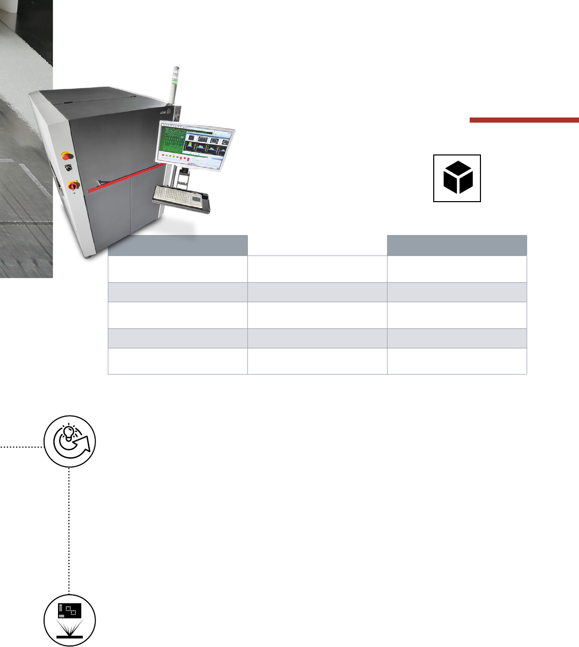
THE HARDW ARE: ASM ProcessLens The core component of the ASM ProcessExpert is the ASM ProcessLens 5D inline SPI system. Instead of operating with rigid piezo-controlled grids, this high-precision, extremely fast SPI syst…
DLP chip Grid with piezo technologies
Flexible patterns for
each image
Band structure Rigid
Projection of dierent patterns Motion Mechanical grid movement
Repeatable imaging Motion accuracy
Mechanical movement
with error risks
Fast Movement speed Slow
Vibration-free electrical swit-
ching
Vibration Vibration caused by actuators
ASM ProcessLens
THE COMPARISON
NEW PRODUCT INTRODUCTIONS (NPIs)
Even experienced experts must often run many test prints to determine the right combina-
tion of printing parameters for a stable printing process. Unfortunately, such experts aren't
always available.
The ASM ProcessExpert operates with the experience of all printing cycles that have
been recorded in its database – around the clock and without overlooking even the
smallest detail. The expert system changes printing parameters in a targeted manner and
nds for each new product the optimal settings after only a few prints.
Your benets: The ramp-up process is shortened dramatically, making NPIs much more
predictable. Your company meets its deadlines more eectively, and throughput rates are
high from the start.
VIRTUAL PRINTS: DFM HEALTHCHECK
A scenario that strikes fear in electronics manufacturers and developers: The stencil for a
new product was delivered, but on the line it turns out that its design or the selected pro-
cess parameters (solder paste type, stencil material, etc.) don't allow for a stable printing
process.
The ASM ProcessExpert provides the solution: DFM HealthCheck with virtual prints
(DFM = design for manufacturability). This function of the expert system simulates the
printing processes exclusively on the basis of the stencil Gerber data, highlights critical
areas, and determines process and printing parameters that are suitable for a stable
process – long before the rst board enters the line.
Your benets: You can check the stencil and process design long before the production
run starts without incurring any costs for prototypes, etc. You can determine the right
process parameters from the start on the basis of the stencil’s Gerber data and prepare
your lines accordingly.
ASM ProcessLens
The extremely fast and
precise 5D SPI system
Traditional SPI system
5
THE HARDWARE: ASM ProcessLens
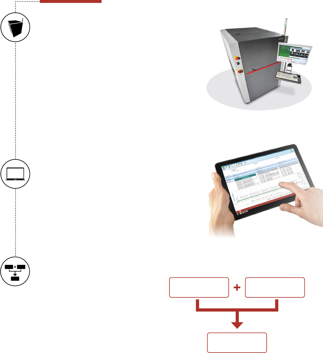
The core component of the ASM ProcessExpert is the
ASM ProcessLens 5D inline SPI system. Instead of operating
with rigid piezo-controlled grids, this high-precision, extremely
fast SPI system is fully digital and generates the Moiré pattern
projections needed to measure the solder paste deposits exibly,
precisely and extremely quickly via a projector chip with 8 million
individually controllable micro-mirrors.
Other advantages include combined 2D/3D measurements, an
X/Y camera positioning system with an accuracy of 12.5 µm, mul-
tiple light sources for shadow-free measurements, 3D-on-the-y
compensation of board warpage, and extremely powerful image
analysis algorithms.
The bottom line: The ASM ProcessLens detects the position,
height, area and volume of solder deposits as well as any PCB
warpage faster and more accurately than traditional SPI systems.
THE SOFTWARE: ASM ProcessEngine
The system combines the measurement data collected by the
ASM ProcessLens with all relevant printing process parameters
and stores them in the database of the ASM ProcessEngine
expert system software. This software learns with each printing
cycle, identies trends and determines corrective measures to
keep the printing process stable within its process window at all
times. The ASM ProcessEngine can output its corrective measu-
res as assist requests or set the new printing parameters directly
on the printer with no human interaction.
FROM SPI TO EXPERT SYSTEM
Thanks to its modular structure, the
ASM ProcessExpert features maximum
investment protection. You can start out with the
ASM ProcessLens as a powerful SPI system and
add the ASM ProcessEngine software later to
expand it into a full-featured expert system.
ASM ProcessExpert
THE MODULAR SYSTEM FOR MAXIMUM
INVESTMENT PROTECTION
ASM ProcessExpert
Expert system
ASM ProcessLens
SPI
ASM ProcessEngine
Software
6

ASM ProcessExpert
THE MODULAR SYSTEM FOR MAXIMUM
INVESTMENT PROTECTION
ASM ProcessLens
TECHNICAL DATA
ASM ProcessLens coverage area
Length – in PCB conveyor direction 1,130 mm
Width 1,300 mm
Height with a conveyor height of 950 mm 1,600 mm
ASM ProcessLens transport
Duration of loading/unloading – single conveyor
Duration of loading/unloading – dual conveyor
Less than 2.5 sec.
0 sec.
Transport height/interface SMEMA, IPC-HERMES-9582
ASM ProcessLens PCB
PCB size (L x W) – single conveyor
PCB size (L x W) – dual conveyor (standard)
PCB size (L x W) – dual conveyor (in single-conveyor mode)
Minimum Maximum
50 mm × 50 mm 610 mm × 560 mm
50 mm × 45 mm 375 mm × 260 mm
50 mm × 45 mm 375 mm × 460 mm
PCB thickness 0.5 mm to 4.5 mm
Minimum edge clearance 3 mm
Maximum PCB weight 3 kg
PCB warpage -7.5 mm to +7.5 mm
ASM ProcessLens inspection values
Pixel size 15 μm × 15 μm
Inspection speed Up to 30 cm
2
/sec
Height resolution 0.37 μm
Height accuracy with calibration target ≤ 1 μm
X/Y gantry accuracy ± 12.5 μm (at ± 3σ)
ASM ProcessLens solder paste inspection
Measurement Shadow-free
Solder paste measurements
Volume, area, height, X- and Y-offset,
shape, bridging, coplanarity
Maximum paste height 1,000 μm
Minimum paste deposit size 90 μm × 130 μm
GRR on printed board << 10%
7