FA1116_datasheet_eng_20191022H.pdf - 第3页
3 The F A1 1 1 6 - 03 can be used i n conjunction with t he U A 1 78 2, which suppor ts boa rds with embedde d passiv e and act iv e devices , to facil itate repai r wor k. Su ppor t for n ot only the F A1 1 1 6 - 03 , b…
2
Reduced-impact link probes
CP1072-01
(option)
High capacitance measurement resolution of 5
aF (1 aF = 10
-18
F)
Capacitance measurement master creation
algorithm
Laser Hight-adjustment unit
FA1950-06(option)
Reduced fine pattern test times
Optional functionality for enhanced capability
Improved front cover for more efficient use
By combining newly designed reduced-impact probes and
precision soft-landing control, the FA1116-03 makes it possible
to approach the maximum speed setting during fine pattern
testing.
Stable, high-resolution measurement ensures that fine pattern
defects such as standalone pads are detected. Since capacitance
values are displayed directly, differences from the reference
board can be easily identified.
A proprietary algorithm designed by Hioki to keep defective
boards from being sent on to the next manufacturing process
aids in the creation of capacitance master data, which can be
created from a single known-good reference board.
Large testing area
The 610 (W) × 510 (D) mm testing area can accommodate
everything from small pieces to large-format boards.
Support for 10 mm probe-up height
Thick ceramic boards and probe cards can be easily positioned
in the tester.
Vacuum suction for easy board clamping
A vacuum suction system is used to clamp the board under test.
Even thin boards and round boards can be clamped with ease.
High-speed image processing system
A new image processing driver (with Windows 7 support) speeds
alignment, reducing test time.
The laser board thickness compensation unit checks the height
of the testing surface at the start of automatic testing to reduce
the effect of differences in board deflection and thickness on
probe impact. Probe damage caused by a failure to properly
clamp the board can also be prevented.
The FA1116-03 delivers continuous testing of a 15 μm fine
pattern at 50 points/sec. (0.03 mm movements, simultaneous use
of two arms, capacitance measurement).
■
MLCC Measurement Unit 1937-40
A dedicated multi-layer ceramic capacitor (MLCC) mode
allows JIS-compliant measured value acquisition.
■
Insulation Measurement Feature 1938-10
A high-speed insulation test function operates at up to 500
MΩ/250 V. Arc detection support is also available on a
special-order basis.
■
Blue Coaxial Downward Illumination Unit 1945-70
The FA1116-03’s coaxial downward lighting uses blue
LEDs to provide effective lighting of ceramic and glass
boards.
■
Dot Marking Function FA1941-01
The FA1116-03 uses oil-based ink to create marking dots
with a diameter of 2 mm. It can also mark CSPs and other
small pieces.
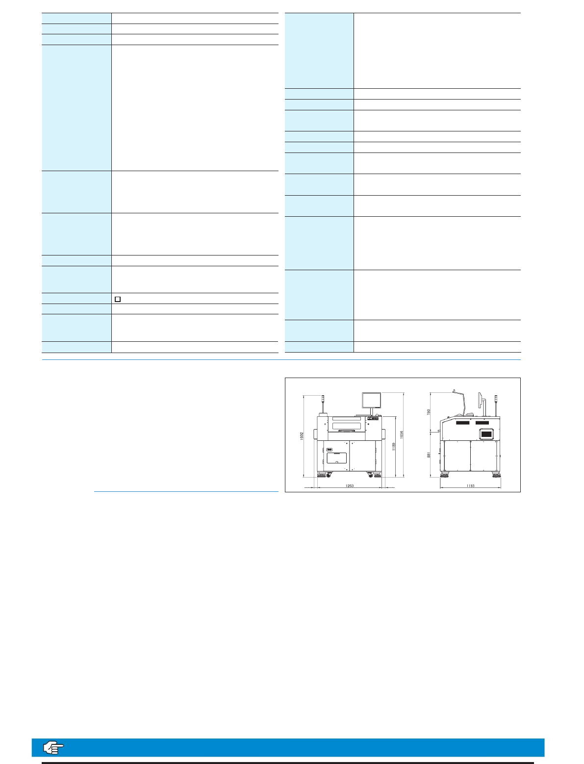
The size of the opening on the front of the tester has been
increased by 30%. Increased rigidity and a large handle make it
easy to open and close the cover quickly.
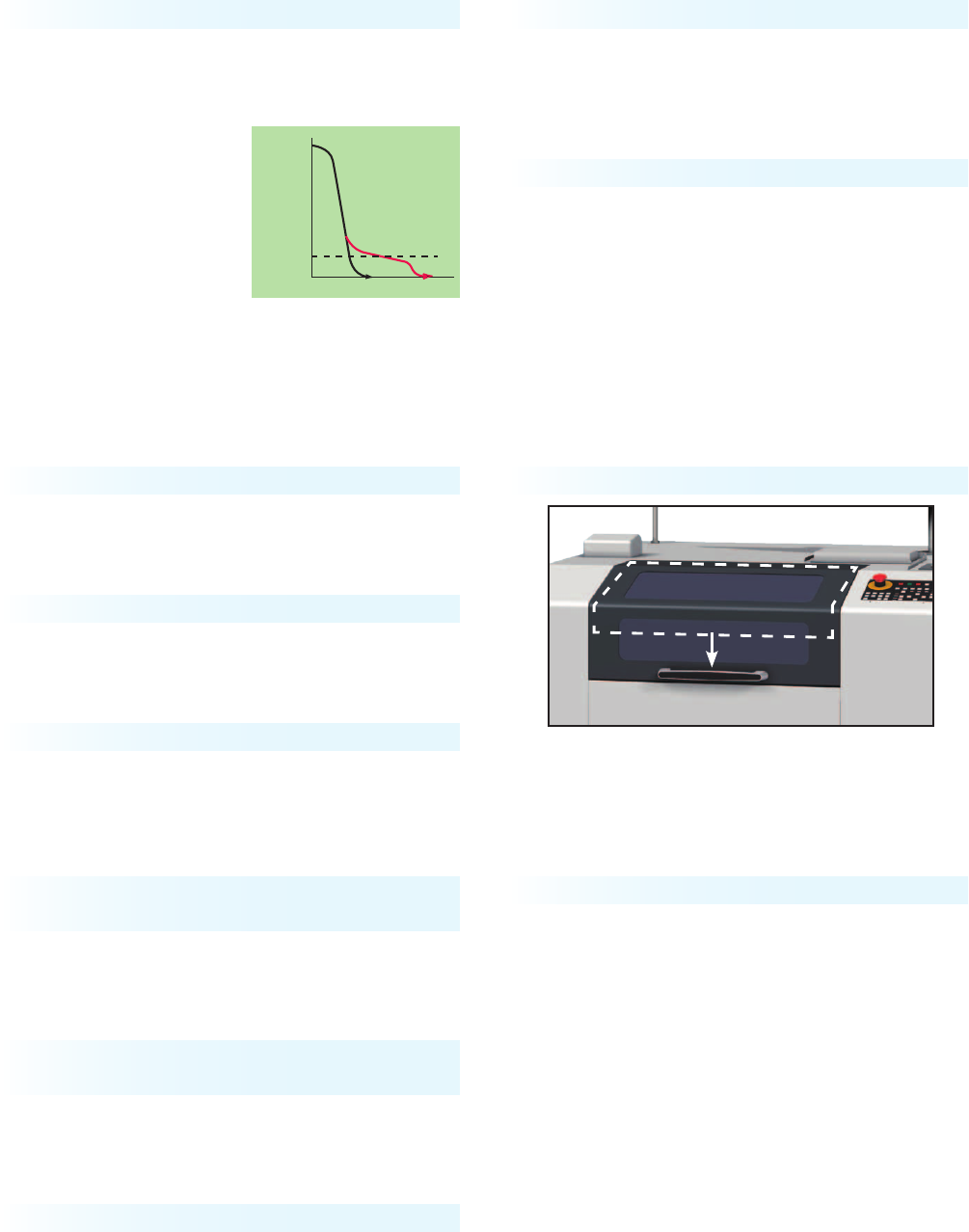
Precision soft-landing function
Probes are lowered at high speed.
Then, just before they come into
contact with the pattern, the motor’s
acceleration is controlled in an
optimal manner to lessen the force
of impact at contact.
Featuring newly designed probes and precision control for
half the impact mark depth of previous designs
*
Rapid testing, regardless of board type
Previous size
The Z-axis descent speed for gold plating and fine pattern testing can be set higher than with
previous models.
Easily position the target board and start testing, even for thin-film boards and thick,
round boards.
Extensive measurement functions and optional units reduce backlogs of untested boards.
*Compared to the C HiTester 1116.
Distance (D)
Board
surface
Time (T)
Soft landing
3
The FA1116-03 can be used in conjunction with the UA1782, which supports boards with embedded passive
and active devices, to facilitate repair work. Support for not only the FA1116-03, but also all Hioki electrical
testing systems, including the FA1282, C HiTester 1116, and 1230 series (designed for mass-production testing),
makes it easy to build a bare board testing system.
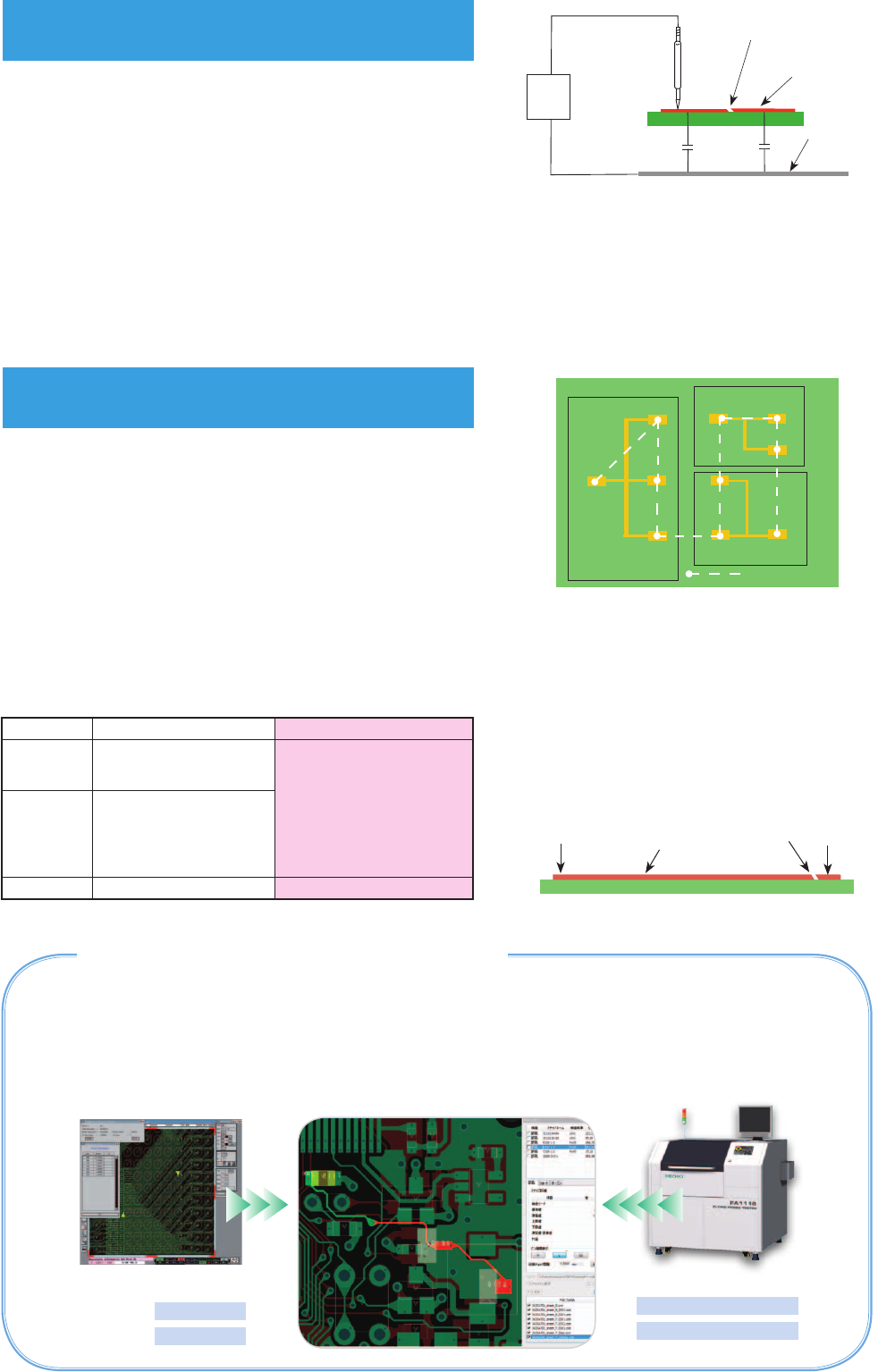
High-speed pattern testing using
capacitance measurement
Methods for calculating the number of test
steps
Any given pattern on the board under test will have a certain
capacitance relative to the electrically isolated test electrode, and
that capacitance is proportional to the area of the pattern. Any
short or break in the pattern will cause a corresponding change in
the area of the pattern, with a resulting change in its capacitance
value. By comparing the measured value to data for a known-
good reference board, it is possible to detect pattern shorts and
breaks. Since capacitance values can be read directly, judgments
can be made based even on minuscule changes in the capacitance.
Furthermore, the FA1116-03’s master extraction algorithm allows
the same approach to be used without regard to board type, from
single-sided glass boards to multi-layer and high-density boards.
In continuity testing, testing for breaks in pattern A require three
test steps: (1)-(2), (1)-(3), and (1)-(4). Similar tests are required for
patterns B and C. Furthermore, when testing for shorts between
patterns A, B, and C, it is necessary to test A-B, A-C, and B-C.
As the complexity of the circuits increases, an enormous number
of test steps become necessary. In testing using capacitance
measurement, it is possible to test for both breaks and shorts with
the minimum number of test points and arm movements since
only the endpoints of each pattern need to be tested.
If there is a break near the end of a pattern as
shown below, the capacitance at point B will vary
significantly, even though the capacitance at point A
varies only slightly. In this way, the break can be
reliably detected.
Capacitance value with no break: CX = CX1 + CX2
Capacitance value with break: CX = CX1
With a break, the detected capacitance value is less than
the corresponding value for the known-good reference
board. With a short, the capacitance value increases by
the capacitance of the other pattern.
Location of break
Cx1
Cx
Cx2
Pattern
Test
electrode
Fail Visualizer UA1782 for repair work
C
Capacitance test route
B
A
(4)
(2)
(3)
(1)
A
B
Break
Pattern
Comparison of test steps
For 100 nets and 500 total endpoints
Resistance measurement Capacitance measurement
Testing for
breaks
All nodes on same net
500 - 100 = 400
Detection of breaks and
shorts using capacitance
measurements for all
endpoints
500
Testing for
shorts
nCr =
100
C
2
100 × (100 - 1) / 2 = 4,950
Total steps 5,350 500
EPA-LINE
Barcode scanning
FLY-LINE
Real-time monitoring
UA1782 Fail Visualizer
Simultaneous display of components and patterns
Importing of display databases Importing of fail results
*Air is required when using the stamp unit.
External dimensions
● Factory options
1355-01 VACUUM PUMP (AC200 V, three phase)
1937-40 MLCC MEASUREMENT UNIT
1938-10 INSULATION MEASUREMENT FEATURE
1945-61 COAXIAL DOWNWARD ILLUMINATION UNIT for 2 ARM
1945-70 BLUE COAXIAL DOWNWARD ILLUMINATION UNIT for 2 ARM
1945-23 BLUE OBLIQUE ILLUMINATION UNIT for 2 ARM
1947-62 1.2 POWER LENS UNIT for 2 ARM
FA1395 RECOVERY DISC
FA1941-01 DOT MARKING FUNCTION
FA1950-06 LASER HEIGHT-ADJUSTMENT UNIT
● Options
The 1116 does not include a printer. please consult with Hioki regarding availability of English printers.
The Link Probe CP1072-01 is a dedicated option designed specifically for use with the FA1116-03. Please note that it cannot be used with other flying-probe testers.
1172-82 LINK PROBE (Link, high-speed version)
1172-83 DOUBLE LINK PROBE (Double link,35µm between terminals)
1172-92 LINK PROBE (1172-66 SR30)
1172-93 LINK PROBE (1172-81 SR30)
1172-94 LINK PROBE (1172-82 SR30)
1172-96 LINK PROBE WITH BLADE (1172-67 CUSTOM BLADE)
1172-97 LINK PROBE WITH BLADE (1172-80 CUSTOM BLADE)
1172-99 DOUBLE LINK PROBE WITH BLADE (1172-69 CUSTOM BLADE)
CP1072-01 LINK PROBE for FA1116
1134-02 IMPRESSION SHEETS
1196 RECORDING PAPER (25m,10rolls)
1350 OFFSET BOARD (t=2mm)
1350-01 OFFSET BOARD (t=1mm)
Probe work area
No. of arms
610 (24.02 in)W×510 (20.08 in)D mm
2
Decision range setting
-99.9 % to +999.9 % or absolute value
No. of probes
2
No. of test steps
Max. 40,000 (300,000 for continuous testing)
Test ranges
DC measurement function
Resistance :400 µΩ to 40 MΩ
Capacitance :4 µF to 400 mF
Diodes, transistors (VF) :
0 to 25 V
Measurement
ranges
Zener diodes (VZ) : 0 to 25 V
Short circuit :400 mΩ to 40 kΩ
Open circuit :4 Ω to 4 MΩ
Voltage : 0 to 25 V
AC measurement function
Resistance :100 Ω to 100 MΩ
Capacitance :10 fF to 10 µF
Coils :10 µH to 100 mH
Measurement
signal
DC constant voltage : 100 mV/400 mV(2 ranges)
DC constant current :
200 nA to 200 mA(13 ranges)
AC constant voltage : 1 Vrms /10 V peak (2 ranges)
AC frequency :
160 Hz/ 1.6 kHz/ 16 kHz/ 160 kHz
DC voltage measurement : 800
µ
V
to 25
Vf.s.
( 8 ranges )
DC current measurement : 100 nA
to 25 m
Af.s.
( 7 ranges )
AC current measurement : 10
µ
A
to
10 mArms. (4 ranges) for 1 Vrms
: 100
µ
A
/
1 mA ( 2 ranges) for 10 Vpeak
Measurement
time
Min. 0.010 sec.
/
step ( Max. 100 points/sec )
(0.1 mm movement with 2-arm simultaneous probing
during capacitance measurement)
Minimum pad diameter
15 µm
Minimum movement step
XY : 1.00 µm/pulse Z : 6.00 µm/pulse
Minimum
Probing pitch
50 µm
Using a link-type probe.
Proper operation is subject to certain conditions.
Fixed and movable
boards
Thickness : 0.1 to 3.2 mm ( 0.004 to 0.126 in )
External dimensions : 50×50 mm to 610×510 mm
(1.97×1.97 to 24.02×20.08 in)
Component mounting limits :
Upper
surface
- 12 mm : 0.47 in
(
including board thickness)
Lower surface - not possible
Board-carrier
N/A
Operation system
Windows7 32bit
Safety devices
Emergency stop switch, safety cover (of anti-static resin),
interference prevention (stops arms from colliding)
External memory
HDD
Display
17-inch color display
Power supply
200 VAC±10 %(single phase) 50/60 Hz
Power consumption : 3 kVA
Pneumatic system
Primary pressure: 0.5 to 0.99 MPa (dry air)
Air consumption
Max. 0.3 Nl/min.
Operating
environment
Temperature : 23±10 ˚C
Humidity : 75 %rh or less(no condensation)
Atmosphere : Avoid use subject to dust, vibration,
or corrosive gases
Floor strength: at least 500 kg/m
2
Accessories
Thermal mini printer ×1, printer cable ×1, grease ×1,
grease gun ×1, arm offset board ×1, keyboard ×1,
mouse×1, mouse pad ×1, PC accessories ×1, Setup disk×1,
color display (17 inch)×1, power cord (loose ends, 3 m)×1,
spare fuse×1, impression sheets ×1
Unit dimensions
Mass
1000 kg (35273 oz )
FA1116 Specifications
FA1116-03 off-line
1443 (56.81 in)W × 1656 (65.20)H× 1185 (46.65)D mm
1139-03 1116-7x DATA COMPOSITION SOFTWARE
UA1781 FEB-LINE INSPECTION DATA CREATION SYSTEM
UA1782 FAIL VISUALIZER
1330-03 MEASUREMENT SECTION CALIBRATION UNIT
( R:Up to 500MΩ ; C,L:ALL )
1356 MAINTENANCE TOOL SET
1172-66 LINK PROBE (for L and R ARM)
1172-67 DOUBLE LINK PROBE (for L and R ARM)
1172-68 LINK PROBE WITH BLADE (for L and R ARM)
1172-69 DOUBLE LINK PROBE WITH BLADE (for L and R ARM)
1172-74 PROBE FOR CALIBRATION (for L and R ARM)
1172-81 LINK PROBE (Link, high-speed version)
Order code Specication
9090
Call us:400-806-2189