FuzionSC_Platform_brochure.pdf - 第6页
Complete Solutions Complementary T echnologies Innova Direct Die Feeder Specications Max Throughput (uph) Flip Chip: 4,700 for 1mm die Direct Chip: 4,000 for 1mm die Presentation Accuracy (Cpk ~1) X,Y = ± 0.15mm @ 3s / …
Differentiation Through Knowledge
All Markets
Leverage process expertise and years of experience
Advanced Process Lab focused on realizing rapid product introduction, maximizing yield and
optimizing reliability
• Leading-edge, fully equipped laboratory
• Optimized assembly solutions (design, materials, process, pioneering equipment technology)
for new and existing products
• Prototyping and development, rst article build, NPI, volume production
• Design for Manufacture (DfM), Design for Reliability (DfR)
• Research partnerships: industry-leading Consortium, multiple University collaborations
APAS applications since 1990; thousands of platforms, all markets
• Flip Chip in Package
• System-in-Package
• Wafer-Level Packaging
• Embedded
• High-Accuracy Place
• High-Speed Passive
One solution for all advanced packaging application challenges
The precision performance and versatile capabilities of the FuzionSC deliver maximum throughput per oor space for virtually any application. With
an unbeatable combination of speed, accuracy and exibility, FuzionSC will have you well-positioned for your next product.
• Substrate and carrier handling with
precision lifter and vacuum tooling
• Flux dip capability with Linear Thin
Film Applicator (LTFA)
• Supports up to 4 Innova direct die
feeders for multi-die applications
• High-speed passive/SMT device
placement
• Vision algorithms/lighting support
all substrate materials & packages
• Look-before-pick ensures highest
pick accuracy
Flip Chip in Package
• Best accuracy (±10µm) at highest
speed over largest area
• Supports panels up to 610mm x
813mm
• AOI accuracy feedback for
post-process compensation
• Software supports high die count
assemblies
• Precision material handling and
thermal stage options
• Die-level traceability SECS–GEM
Wafer-Level Packaging
• Thin and narrow substrate handling
• Bad circuit detection, electronic
pass-down
• Gang ux dip for maximum cph
• Supports up to 4 Innova direct die
feeders for multi-die applications
• High-density passive placement,
01005 and smaller, 4x1 feeding
• Small ducial & ducial teach-by-
show pattern nd
• Highest speed ip chip placement
System-in-Package
• Best accuracy (±10µm) at highest
speed over largest area
• Panels up to 610mm x 813mm
• Supports high device count, both
passives and actives
• AOI accuracy feedback for
post-process compensation
• Precision material handling and
thermal stage options
• Die-level traceability SECS–GEM
• Top-side alignment (TAP) process
Embedded
• Available dual-beam congurations
with multiple heads
• Up to 14 spindles with gang pick
• Up to 30,750 cph
• 4 x 1mm tape feeders
• High-speed & high-accuracy modes
• Bad circuit detection, electronic
pass-down
• Custom applications tooling:
nozzles, substrate support
• Motion proles for sensitive
device handling
High-Speed Passive
• High speed, high accuracy
• 01005–55mm sq & up to 25mm tall
• Top-side alignment (TAP) process
for LED headlamps, CPV
• Advanced vision algorithms,
programmable 3-axis lighting
• Wafer, tray, tape, tube, and bulk
feeding formats
• Custom applications tooling:
nozzles, grippers, substrate support
• Up to 5000g force, 30 seconds
dwell
High-Accuracy Place
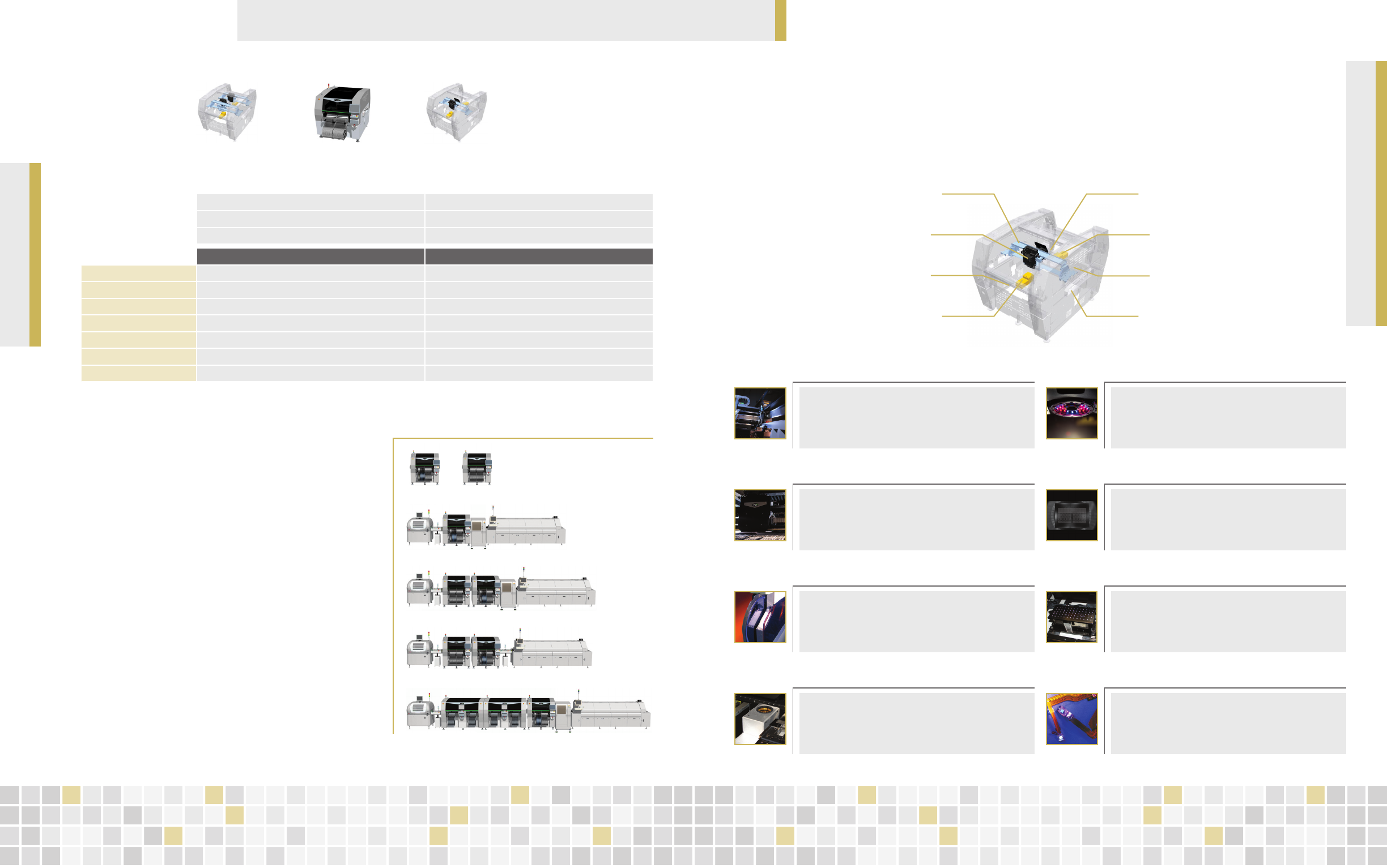
FuzionSC Portfolio & Solutions
Capability Designed In
FuzionSC2-14
For higher throughput requirements
FuzionSC1-11
Lower cost with additional exibility
Dual-beam, dual-drive overhead gantry system Single-beam, dual-drive overhead gantry system
2 FZ7 (7-spindle) placement heads 1 FZ7 (7-spindle) + 1 optional FZ4 (4-spindle) placement head
450ms tact time (w/ ux dipping), 360ms (w/out) 750ms tact time (w/ ux dipping), 600ms (w/out)
FuzionSC2-14 Specications FuzionSC1-11 Specications
Throughput (cph) 30,750 (Max) / 14,200 (4-Bd IPC Chips) 16,500 (Max) / 8,400 (4-Bd IPC Chips)
Accuracy (µm@>1.00 Cpk) ±10 (Array Devices/Flip Chip) / ±38 (Passives/Chips) ±10 (Array Devices/Flip Chip) / ±38 (Passives/Chips)
Max Board Size 508 x 813mm (20 x 32”), larger board specials available 508 x 813mm (20 x 32”), larger board specials available
Max Feeder Inputs (8mm) 120 (2 ULC) 120 (2 ULC)
Feeder Inputs Types Wafer (up to 300mm), tray, tape, tube, and bulk Wafer (up to 300mm), tray, tape, tube, and bulk
Component Range (mm) (0201) .25 x .5 x .15 (Min) to 150 square (MFoV), up to 25 tall (0201) .25 x .5 x .15 (Min) to 150 square (MFoV), up to 25 tall
Min Bump Size & Pitch (µm) Bump Size: 20, Bump Pitch: 40 Bump Size: 20, Bump Pitch: 40
Advanced technologies for advanced applications
FuzionSC features specialized technologies to address leading-edge component packaging challenges.
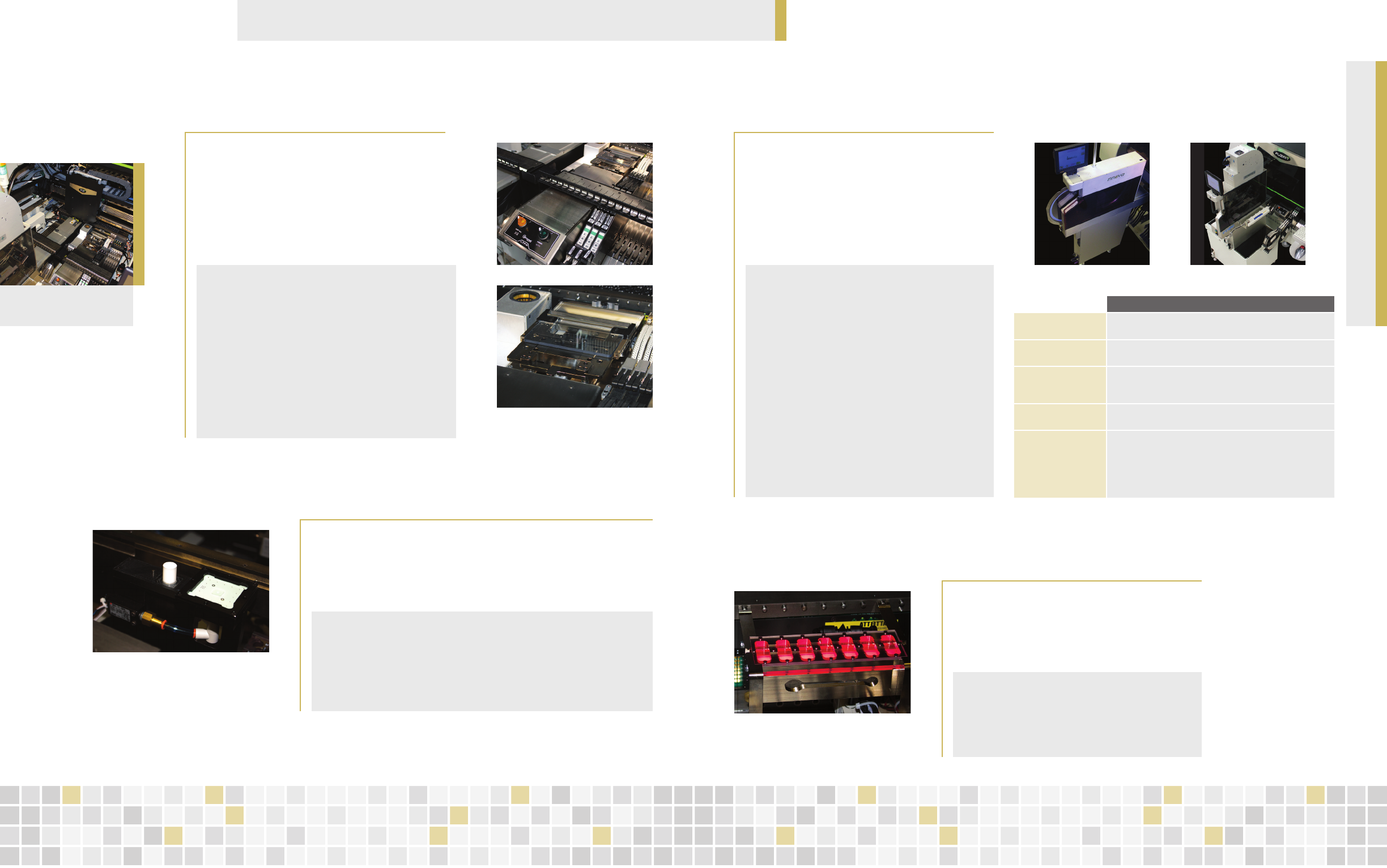
Fast, precise PEC Camera
Advanced vision algorithms
& lighting
Precision lifter & tooling
Versatile substrate handling
VRM Linear Motor
Positioning System
Accurate, exible
FZ™ placement heads
Multiple feeding options for
ip chip, bare die, SM
High-resolution Magellan™
digital cameras
• High-accuracy (1µm resolution), closed-loop positioning
control supports converging & emerging technologies
• High acceleration (up to 2.5G), thermally stable
• Self-correcting, dual-drive control reduces settle times
VRM Linear Motor Positioning System
• High-resolution (.27MPP)
• Programmable lighting, wavelength illumination, cross
polarization
• Standard/taught ducial and pad site recognition
Fast, precise PEC Camera
• Precision accuracy (27µm @ Cpk>1)
• 0201 – 150mm square (MFoV), up to 25mm tall
• High-speed IC and chip, gang pick up to 7 components
• Standard Package-on-Package (PoP) functionality
Accurate, exible FZ™ placement heads
• Front, side, and on-axis combination lighting
• Lighting calibration performed on the machine,
eliminating machine-to-machine intensity variation
• Lighting intensity is consistent across viewable area
Advanced vision algorithms & lighting
• Wafer, tray, tape, tube, and bulk
• Up to 4 direct die feeders, wafers up to 300mm
• Stationary and stackable matrix trays
• Standard and dual-lane tape for small passives
Multiple feeding options for ip chip, bare die, SM
• Handles strips/lead frame, auer boats, carriers/pallets,
boards/panels from 0.10mm – 12.0mm thick
• Integral vacuum generator
• Precise registration of the substrate in x, y and z axis
Precision lifter & tooling
• Supports all ip chip and SM devices
• High resolution of 1024 x 1024 enables small part
feature recognition
• 2.3, 0.94, 0.5, 0.2MPP (supports 20µm bumps/pillars)
High-resolution Magellan digital cameras
• Thin, thick, narrow, and large assembly area
• Substrates, wafers, lead frames, ceramics, glass, ex,
and laminates
• Large substrates up to 625mm x 813mm
Versatile substrate handling
Scalable solutions for cost-ecient productivity
Stand-alone machine solution – All-in-one eciency
Single-beam for high exibility, dual-beam for higher throughput; Wafer, tray, tape, tube,
bulk feeding – Fan-Out WLP, Die Attach, Lid Attach, High-Accuracy Place, Embedded
Mass reow – Full-process, high-mix/NPI
Complete process solution supporting multiple feeding formats and ux or solder paste
dipping – Package-on-Package, System-in-Package, 2.5D, Flip Chip, SMT, Odd-Form
Mass Reow – Scaled assembly, Medium-mix, medium-volume
Complete process solution with dedicated chip placer and exible high-accuracy placer
supporting HVHM tray packaging – High-Speed Passive, High-Accuracy Flip Chip
Mass Reow – Medium to high-volume
Complete process solution with chip placer and high-accuracy placer; higher volume,
same footprint – System-in-Package, High-Speed Passive, High-Accuracy Flip Chip
Mass Reow – Versatile high-volume
High-throughput full process solution with large feeder capacity for streamlined change-
overs – System-in-Package, High-Speed Passive, High-Accuracy Flip Chips, WLP
FuzionSC1-11 FuzionSC2-14
FuzionSC1-11 PTF
FuzionSC1-11 PTFFuzion1-30
FuzionSC2-14Fuzion2-60
FuzionSC2-14 PTFFuzion4-120Fuzion4-120
Complete Solutions
Complementary Technologies
Innova Direct Die Feeder Specications
Max Throughput (uph) Flip Chip: 4,700 for 1mm die
Direct Chip: 4,000 for 1mm die
Presentation Accuracy
(Cpk ~1)
X,Y = ± 0.15mm @ 3s / ±27.0° (veried against 1.0mm die size)
Wafer Specication Maximum Size: 300mm (12”)
Minimum Size: 100mm (4”)
Expansion Depth: 6.35mm, 6.0mm, 0.0mm (unexpanded)
Vision Recognition
Methods
Thresholding, Pattern Matching, Corner Detection, Solder
Bump Detection, Wafer Mapping
Die Specication Minimum Size (L x W): 0.7mm x 0.7mm (0.027” x 0.027”)
Maximum Size: (L x W) 11.0mm x 11.0mm (0.43” x 0.43”)
Minimum Thickness: 75 µm (0.003”)
Maximum Thickness: 4.0mm (0.163” nominal)
Die Material: Silicon, Gallium Arsenide, Ceramic, Glass
Ball Types: Ball bumps, Stud bumps
Linear Thin Film Applicator (LTFA)
On-board dipping for maximum eciency
The Linear Thin Film Applicator (LTFA) creates a thin lm of ux,
solder paste, or adhesive. Flip chips, stacked CSPs and other area
array packages are individually or gang dipped, thereby applying
the necessary amount of material to the appropriate area.
• Linear actuation for thickness uniformity and repeatability
• Gang dipping, up to seven spindles
• Up to two LTFAs per FuzionSC Platform
• Quick-change plates for depth control (no adjustments)
• Typical viscosity 10K – 28.5K centipoise
• Programmable milling cycles
• Programmable dipping dwell time
• Programmable Maintenance Monitor
• Quick-release tooling for easy cleaning
• Large reservoir (up to eight hours run time)
• Dip verication based on spindle impact sensing
• Uses patterned glass plate and glass device to measure and automatically
optimize placement accuracy
• Aligns each individual spindle in x, y and theta
• Ensures sub-micron process repeatability
• User interface displays X, Y oset history
• Activated by time/board number intervals or temperature limits
Accuracy Management System (AMS)
Maintaining the performance you demand
The Accuracy Management System (AMS) combines a hardware station with supporting
software to manage FuzionSC accuracy performance over time.
Innova Direct Die Feeder
Delivering high-speed bare die to the mainstream
Embrace the convergence era of electronics assembly with the
Innova™ and Innova +™ Direct Die Feeders. Innova enables the
presentation of wafer-level devices to Universal’s FuzionSC
Platform without incurring costly packaging charges.
• Presents ip chips and bare die in wafer format for pick
and place
• Enables ip chip, bare die and SMT on a single platform
• Single-wafer feed (Innova), 13-slot cassette wafer-feed
(Innova +)
• Eliminates upstream wafer sorting
• Ideal for SiP applications
• Up to four feeders per FuzionSC Platform
• Processes wafers up to 300mm
• Ink and ink-less wafer map support
• Wafer expansion: programmable (Innova +), xed with
grip rings (Innova)
• Flip and non-ip die presentation support
• Traceability support
• Ideal for NPI or high-volume
• Provides accurate top-side feature alignment through
body-to-feature inspection
• Leverages gang pick and place for speed
• Holds up to 7 components with vacuum
• Field-retrottable option
Precisor Top Feature Inspection Station
Ensuring highest accuracy without compromise
The Precisor™ Top Feature Inspection Station optimizes placement
accuracy by providing a platform for precise device inspection.