Brochure-PacTech-WLP-Services.pdf - 第3页
Advanced Packaging Platforms ENIG UBM for Flip Chip & WLCSP ENEPIG for Wire Bonding Solder Bump for Flip Chip & WLCSP Cu Pillar for Flip Chip & WLCSP Wafer Backside Processing and Die Singulation: Wafer Thinn…
o
Design
&
manufacturing
of
specialized
equipment
for
over
20
years
o
Process
development
&
subcontracting
services
utilizing
leading-edge
technologies
o
Proprietary
chemistries
for
demanding
semiconductor
technologies
o
Partnerships
supporting
global
customers:
IDMs,
OEMs
&
Fabless
Customized
Turnkey
Solutions
Broad
Range
of
Wafer
Level
Packaging
Services:
o
Electrolytic
&
Electroless
Plating
of
UBM
and
Bump
o
Repassivation
Layers
o
Sputtered
&
Electroplated
Redistribution
Layers
(RDL)
o
Solder
Bumping
-
Jetting
&
Ball
Placement
o
Wafer
Thinning
&
Dicing
o
Wafer
Backside
Metallization
o
Die
Sorting
in
Tape
&
Reel
or
Waffle
Pack
Flexible
Operation
Models
o
High
Volume
Subcontracting
Service
o
In-house
Technology
Transfer
using
Paclech
Equipment
o
Second
Sourcing
out
of
Global
Paclech
Locations
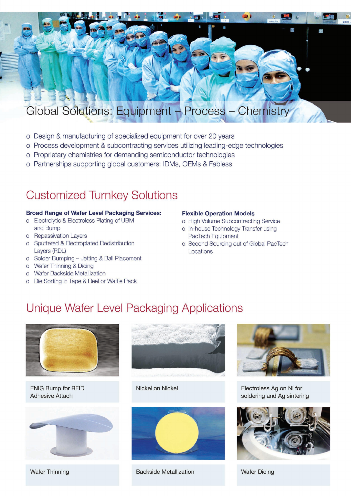
Unique
Wafer
Level
Packaging
Applications
ENIG
Bump
for
RFID
Adhesive
Attach
Nickel
on
Nickel
Electroless
Ag
on
Ni
for
soldering
and
Ag
sintering
Wafer
Thinning
Backside
Metallization
Wafer
Dicing
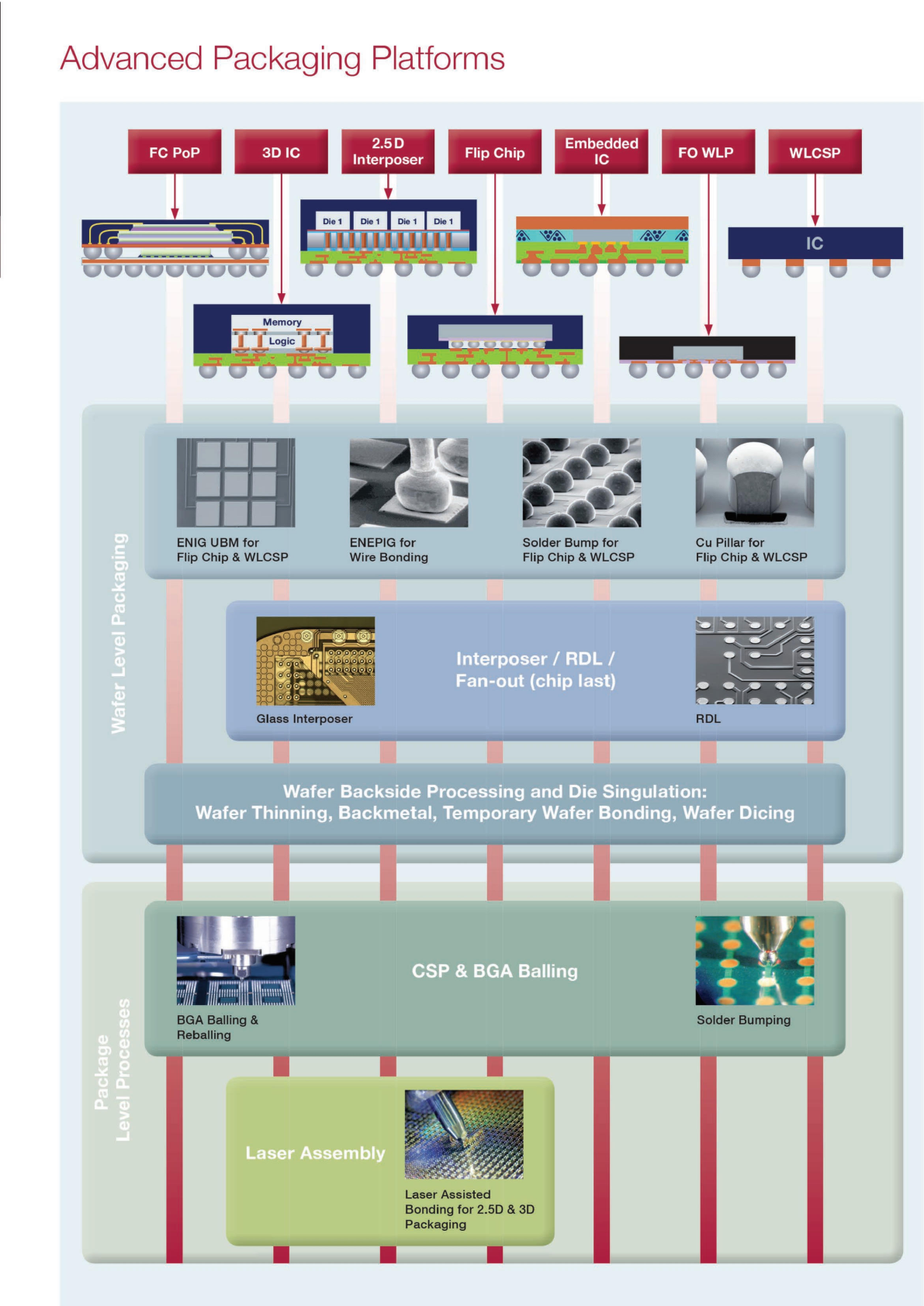
Advanced
Packaging
Platforms
ENIG
UBM
for
Flip
Chip
&
WLCSP
ENEPIG
for
Wire
Bonding
Solder
Bump
for
Flip
Chip
&
WLCSP
Cu
Pillar
for
Flip
Chip
&
WLCSP
Wafer
Backside
Processing
and
Die
Singulation:
Wafer
Thinning,
Backmetal,
Temporary
Wafer
Bonding,
Wafer
Dicing
o
>3
a>
JeM
sess
<D
sexoed
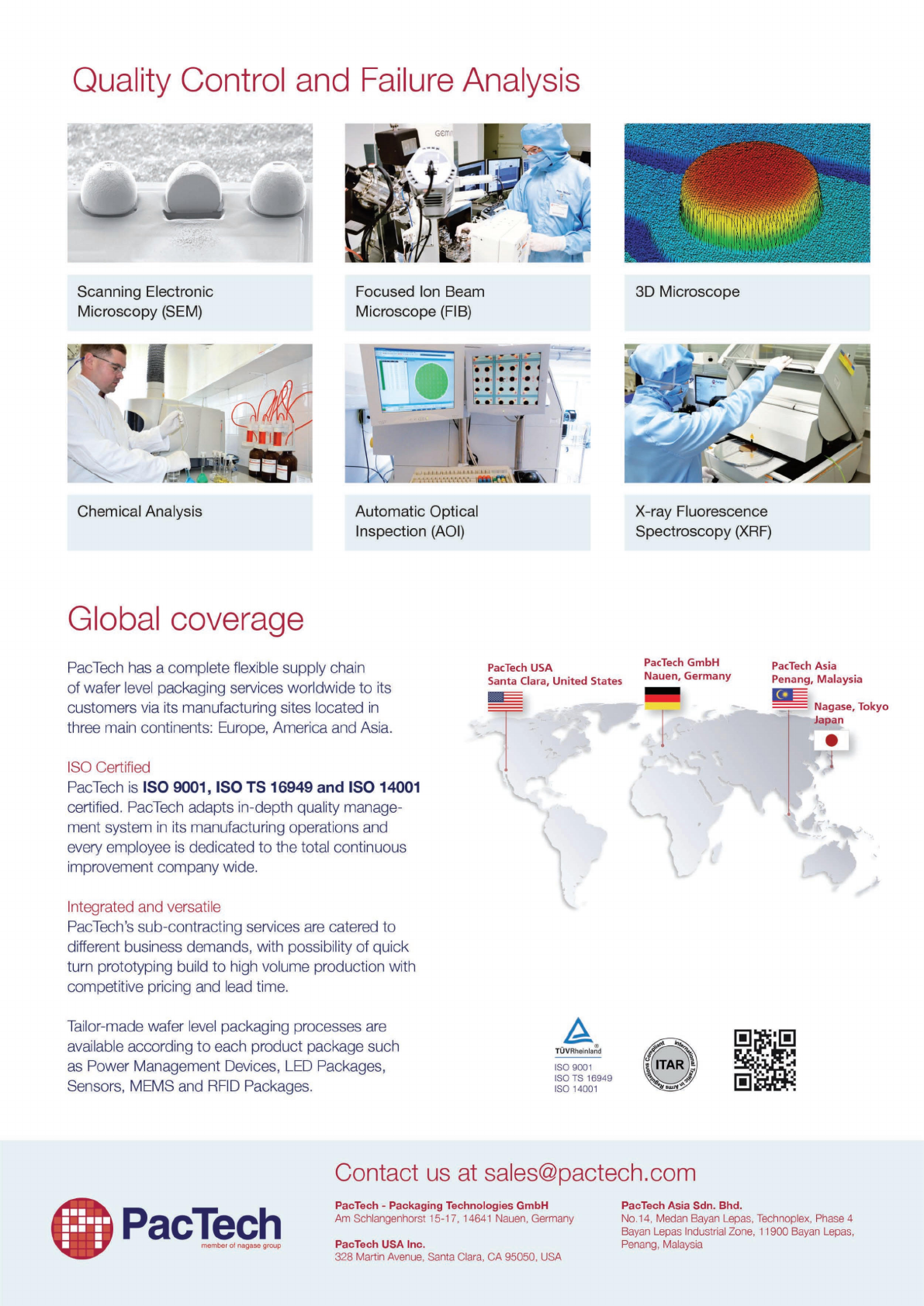
Quality
Control
and
Failure
Analysis
Scanning
Electronic
Microscopy
(SEM)
Focused
Ion
Beam
Microscope
(FIB)
3D
Microscope
Chemical
Analysis
Automatic
Optical
Inspection
(AOI)
X-ray
Fluorescence
Spectroscopy
(XRF)
Global
coverage
Paclech
has
a
complete
flexible
supply
chain
of
wafer
level
packaging
services
worldwide
to
its
customers
via
its
manufacturing
sites
located
in
three
main
continents:
Europe,
America
and
Asia.
ISO
Certified
Paclech
is
ISO
9001,
ISO
TS
16949
and
ISO
14001
certified.
Paclech
adapts
in-depth
quality
manage¬
ment
system
in
its
manufacturing
operations
and
every
employee
is
dedicated
to
the
total
continuous
improvement
company
wide.
Integrated
and
versatile
PacBch's
sub-contracting
services
are
catered
to
different
business
demands,
with
possibility
of
quick
turn
prototyping
build
to
high
volume
production
with
competitive
pricing
and
lead
time.
Tailor-made
wafer
level
packaging
processes
are
available
according
to
each
product
package
such
as
Power
Management
Devices,
LED
Packages,
Sensors,
MEMS
and
RFID
Packages.
Paclech
USA
Santa
Clara,
United
States
Paclech
GmbH
Nauen,
Germany
PacTech
Asia
Penang,
Malaysia
Nagase,
Tokyo
Japan
A
TUVRheinland
ISO
9001
ISO
TS
16949
ISO
14001
曲
Paclech
member
of
nagase
group
Contact
us
at
sales@pactech.com
PacTech
-
Packaging
Technologies
GmbH
Am
Schlangenhorst
15-17,
14641
Nauen,
Germany
PacTech
USA
Inc.
328
Martin
Avenue,
Santa
Clara,
CA
95050,
USA
PacTech
Asia
Sdn.
Bhd.
No.
14,
Medan
Bayan
Lepas,
lechnoplex,
Phase
4
Bayan
Lepas
Industrial
Zone,
11
900
Bayan
Lepas,
Penang,
Malaysia