PI series 3D SPI brochure and specifications.pdf - 第2页
Goodb y e de f ect s . Hel l o sol der pas t e perfectio n . What a re the most common d efects in your S MT line? And what would you save if you could catch the m earlier in your p rocess—or ev e n eliminate them f ro…
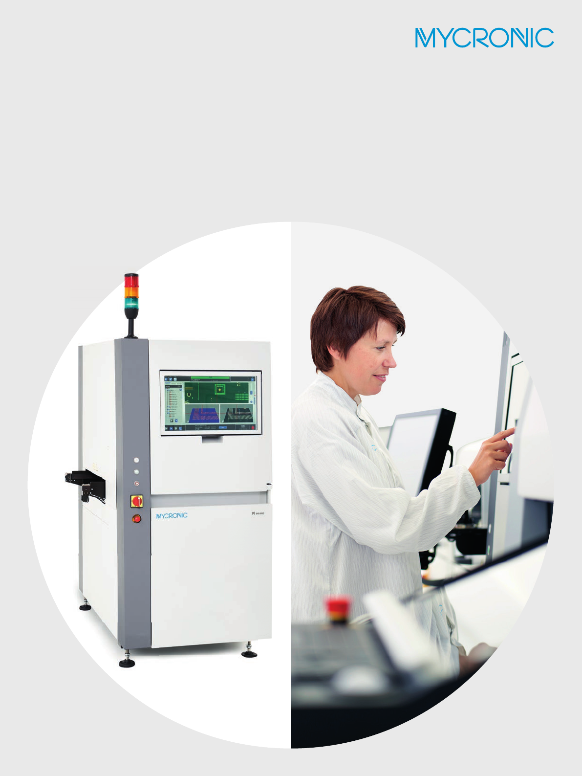
Accurate solder paste inspection
with unprecedented simplicity
Mycronic inspection solutions PI
™
series 3D SPI
Goodbye defects.
Hello solder paste perfection.
What are the most common defects in your SMT line? And what would you save
if you could catch them earlier in your process—or even eliminate them from
your design altogether?
If you’re like most manufacturers, the answers
to these questions will likely bring you back to
the solder paste printing process. Because this is
where more than 60% of all SMT defects originate,
according to our latest industry survey. Whether
theproblem is solder shorts or insucient solder
paste deposits, accurate solder paste inspection is
often the most economical way to detect, predict
and prevent defects before they occur.
As solder paste deposits continue to decrease in
size, the value of advanced SPI analysis will only
grow over time. This is precisely what makes the
innovative PIseries 3D SPI system an increasingly
critical part of acomplete metrology solution.
It allows you to measure paste volume with un-
matched accuracy and unprecedented simplicity.
Sothat you can continually improve your process
and tolerance settings—and take advantage of
theunambiguous real-time information you need
to take your yield to new heights.
It’s one more part of the Mycronic4.0
intelligent factory, and one step
closerto perfection.
3
PI series 3D SPI
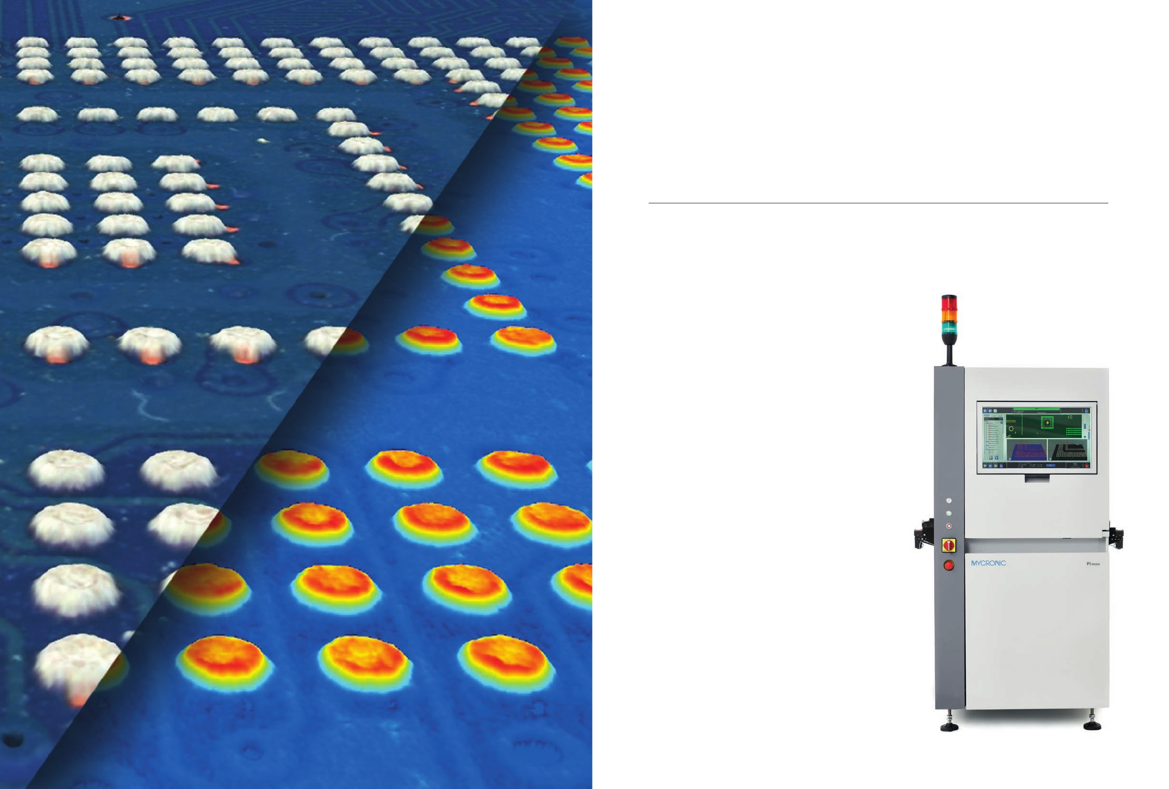
Perfect solder joints
madesimple
Measure paste volume with extreme precision. Improve your
process and tolerance settings with automatic pad grouping.
And monitor your process in real-time, both online and o ine.
The PI series gives you highly accurate SPI data, combined
with a range of smart auto-programming functions that ensure
high-quality inspection regardless of operator experience.
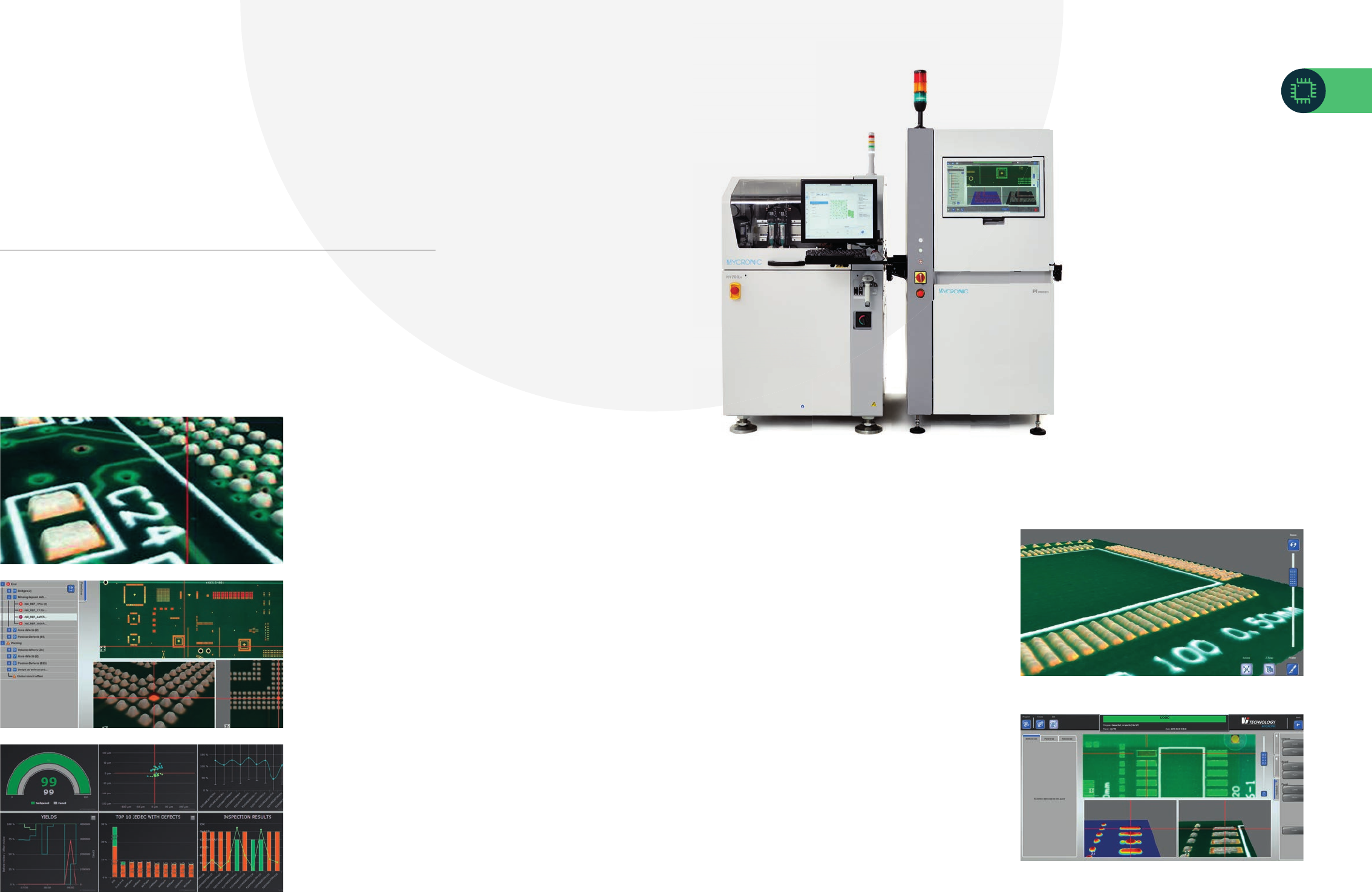
INSPECTS JET-PRINTED PCB
WITHTHE SAME VIRTUOSITY
In line with the evolution of SMT manufacturing
practices, the PI series handles jet-printed PCBs with
the same inspection performances and program-
ming process as for screen-printed boards. Thesyn-
ergy with Mycronic MY700 Jet Printer enables the
inspection of all types of deposit shapes and vol-
umes, regardless of the type and viscosity ofthe
jetted paste.
Extreme inspection precision
PI series 3D SPI accurately calculates the expected
volume of paste printed by the MY700 Jet Printer.
Instead of evaluating this volume based on the
Gerber stencil data, PI series uses data transmitted
from the MY700 Jet Printer.
PI series MY700 repair loop
PI series communicates any defects resulting from
insu cient paste to the MY700, along with the
IDcode of the concerned PCB. A second run in
thejet-printer corrects the defect without having
towash and reprint the entire board.
Accurate Z-referencing technology
Captures hundreds of references across
anultra-large 55x350mm 3Dfi eld of view.
PI series 3D SPI verifying paste defect has been
corrected by the MY700 Jet Printer.
Simple auto-programming
Ensure high-quality inspection regardless of
operator experience with the industry’s only
auto-programming SPI.
Repeatable process results
Unique warp compensation delivers
accurate measurements in real production
environments, with nofalse calls.
Inspection of jetted paste deposits.
MY700 Jet Printer
and PI series 3D SPI.
MY700 Jet Printer combined
with PI series 3D SPI provides
near zero-defect solder
paste printing process.
4 5