SMTAi Paper_Printing Small Aperture components Final Aug_2_2019.pdf - 第2页
Printed Circuit B oards (PCB) : As Process Engineers, most PCB d esigns are created long before we beco me involved. Design for manufacturing considerations are most often out weighted b y cost requirements. We are often…
STENCIL PRINTING 008004/0201 APERTURE COMPONENTS
Edward C. Nauss and Michael Butler
ITW EAE
Hopkinton, MA
enauss@itweae.com; mbutler@itweae.com
ABSTRACT:
This paper will focus on the application requirements of
solder printing small aperture designs, concentrating on
008004 (inch) / 0201 (metric) size components, and the
results of a design of experiment printing these challenging
apertures. As Moore’s law continues to be applied to
component miniaturization, the next installment of reduced
packaging has arrived in the form of the 008004/0201 for
resistors and capacitors. Component size roughly the size of
a grain of sand presents specific challenges to the solder
printing process. To address these challenges, each aspect of
the printing process will need be examined. This includes
essential machine requirements, including correct squeegee
blades, tooling support, and calibrations, to meet the
demanding specifications. The correct match and design of
materials will be addressed, focusing on the stencil and
substrate design along with solder paste and cleaning
solvent requirements. A design of experiment will be
reviewed that applies the machine and materials discussed,
including the printer and Solder Paste Inspection (SPI) setup
and the specific machine parameters used. The results of
these DOE’s will then be closely examined.
Key words: printing, miniaturization, component, stencil,
solder paste, 008004, 0201mm
BACKGROUND:
Moore’s Law states that the number of transistors a
microchip can contain is expected to double every two
years. The same trend can be applied to miniaturization of
components. Demands for high functionality from mobile
devices, smart watches, wearables, military, medical and
audio technology continues to drive the development of
component miniaturization. The SMT industry has seen the
introduction of the next generation of component
miniaturization every 4-7 years with the latest release of the
008004” (0201mm) component size. With a 6% reduction of
area and a 1.6% reduction in volume when compared to a
01005” (0402mm) package size, the equipment
manufacturers have quickly adapted to this next challenge.
However, when introducing micro devices to a
manufacturing process, the problematic hurdle that needs to
be addressed is the printing process. Focus on the materials,
machine and process that ties them together, needs to be
addressed in order to successfully introduce 008004”
(0201mm) components into a manufacturing process.
Developing a process that can produce a product containing
008004” (0201mm) with a Cp value that is twice a capable
can be achieved when each element of the process is
working together. This will require the engineer to
reevaluate their present process to adapt to the challenges
this component will require in order to successfully
implement a 008004” (0201mm) component. This may go
as far as implementing a clean room environment. The focus
of this paper will be on the individual elements of the
printing process and the results of testing performed at the
ITW EAE process lab in Hopkinton, Massachusetts.
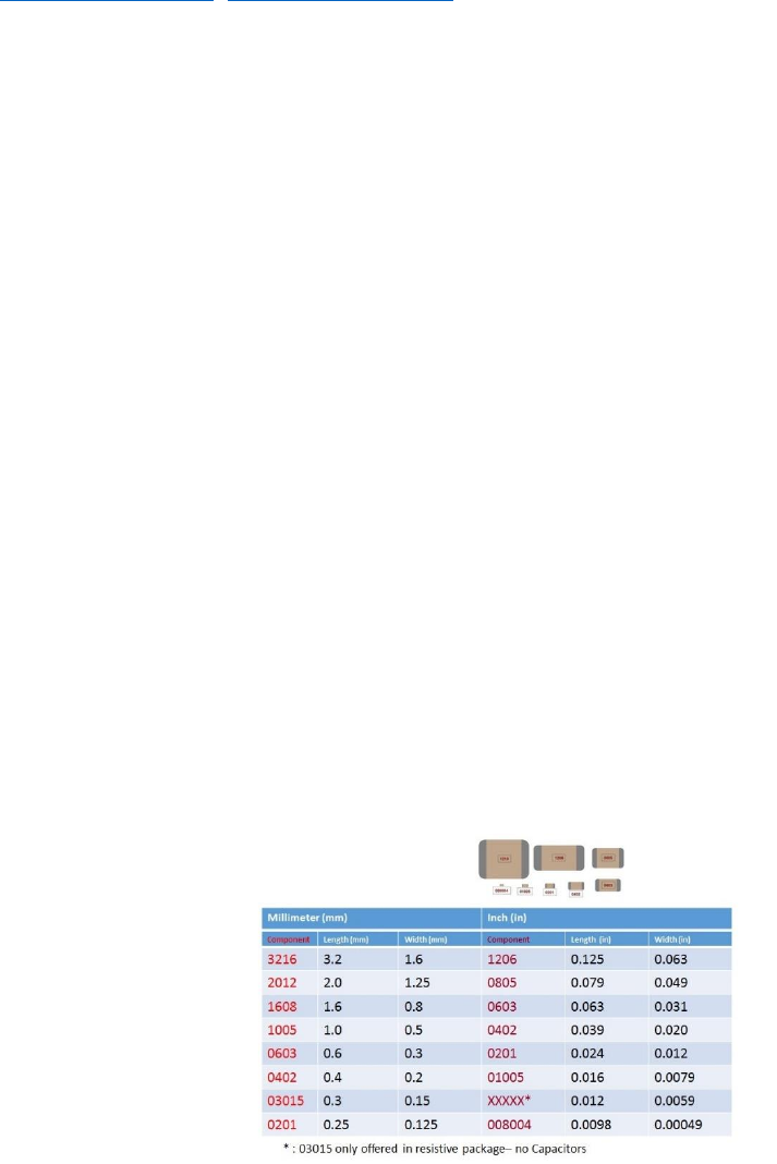
Status of components today:
Referencing (Figure 1) most of the market has become
comfortable with products that contain components down to
0402” (1005mm). Recently 0201” (0603mm) components
are becoming more common in mass production with the
01005” (0402mm) just now entering the mainstream. With
each step, we have adapted stencil designs and materials to
implement these components into our designs with little or
no consideration to the other key elements. Printing
008004” (0201mm) requires us to examine each element of
the process prior to fabricating our first substrate to insure
each element is designed with this component challenge in
mind. The solution to micro component printing is in the
aggregate, where each element is using best practices for
optimum results. Any deviation or ignoring any element
will result in a less than repeatable process.
Figure 1: Component sizes
Printed Circuit Boards (PCB):
As Process Engineers, most PCB designs are created long
before we become involved. Design for manufacturing
considerations are most often out weighted by cost
requirements. We are often faced with having to design the
process to the board rather than the other way around where
adjustments and compromises are made to accommodate
shortfalls in the PCB design. This is where the Process
Engineer needs to take an active role to make sure that
success is designed into the PCB to insure repeatable
results. So far, applications have been focused on micro
components with little to no mixed technology on multi-up
panels. The problems with mixed technology, also referred
to as the broadband printing issue, is not the focus of this
paper though this would need to be addressed before
proceeding. Most applications to date have been using PCB
thicknesses of 0.030” (0.762mm) or less, so this should be
expected. Based on the PCB thickness and the amount of
routing, special carriers maybe needed to transfer the
product from machine to machine as well as stabilize it
during the reflow process. One of the key elements to
successful printing which the PCB plays a major role is the
capability to form a seal between the stencil and the PCB
commonly referred to as gasketing. Gasketing in turn plays
directly into the process to transfer the paste from the stencil
aperture to the PCB pad efficiently and repeatably.
Maintaining a consistent board thickness, by elimination of
variance in mask thicknesses from PCB to PCB, is key as
this determines the position of the PCB to the bottom stencil
surface. Mask encroachment on to the pad surface should be
eliminated as this will greatly affect the capability to seal
the aperture. Nomenclature and silk screens should be
avoided in the PCB design. Issues arise when silkscreen is
equal to or greater than the stencil thickness being applied
along with being located adjacent to the component. Logos
and identification information should be presented on the
back of the PCB or located in consideration to cause the
least effect on the critical components. The use of barcode
labels should be avoided as this is the source of many
printing issues with less challenging components. Barcode
labels should be applied after the print process is completed
if possible. One of the critical mistakes when designing
PCBs for micro component printing is to make sure the pad
is not significantly below the mask height. When designing
a board with a bare copper pad, the pad should be just below
or equal to the mask height. If the pad is below the mask,
this creates a gap that the paste must now overcome when it
is printed into the aperture. Because the paste must flow
between the aperture opening on the bottom of the stencil to
the pad surface, the paste will be unable to secure a proper
adhesion to pad surface. The result is erratic print results
that is represented in opens and insufficient volume or pad
coverage. In some cases, the PCBs with this issue become
non-manufacturable due to erratic results from the printer.
To insure the pad is positioned correctly to the mask height
and has a flat planar surface, an electroless nickel
immersion gold (ENIG) plating should be considered. ENIG
plating, consisting of an electroless nickel plating covered
with a thin layer of immersion gold, protects the nickel from
oxidation has shown to have the best results. In the board
design, the decision to use mask defined pads often present
issues. Accuracy of the pad locations as well as pads that are
sized larger than the specification have been issues when
using mask defined pads. Location of the fiducials,
especially when implementing a multi-up panel, is critical
for the machine vision systems to properly perform
alignment. The fiducials should be part of the artwork and
be present on the PCB image for best results. Avoid locating
the fiducials on the breakout panel as this tends to add to
any alignment error. Stretch and step and repeat errors
should be avoided as we are dealing with a recommended
pad size of 0.005” X 0.006” (0.127 x 0.1524mm) where as
much as a 0.001” (0.0254mm) error can have significant
consequences. Investment up front in the PCB design and
manufacturing will insure success where some of the
previously described issues are often difficult if not
impossible to overcome.
Squeegee Blades/Enclosed Heads:
A best practice is to separate a set of squeegee blades
specifically used for micro-component printing. This insures
that the blades being used are undamaged and not worn. The
squeegee requirements for micro-component printing is
simple, spring steel blades with a squared edge is all that is
required. A blade angle of 55 degrees is also recommended
where standard blade angles are set to 60 degrees. This
change in angle allows more surface area of the blade over
the aperture to promote an improved aperture fill. It also
improves sheering off the paste at this angle when the blade
passes over the aperture to prevent paste drag out and erratic
aperture fill. Blade length should match the PCB as closely
as possible with a maximum size range within 2 inches of
the PCB size in X direction. This will center the squeegee
pressure on the PCB as well as prevent long term damage to
the stencil. Inspect the blades every time prior to use for
cleanliness and for damage. It should be noted that enclosed
heads have been used for fine featured printing applications
with great success in the market today. The extrusion flow
from the pressurized chambers are compatible for repeatable
aperture fill for micro-component printing. Some Type 6
pastes have a limited stencil life where enclosed chambers
address this issue and minimizes paste waste. For this test
we focused on squeegee blades as this represents most of
the process applications on the market.
Stencils:
For this experiment we used a 29” x 29” (736 x 736mm)
fine grain, laser -cut, Nano-coated, 0.002” (0.0508mm)
thick stencil. The aperture size is a square, 0.005” x 0.006”
(0.127 x 0.1524mm) that is one to one with no reductions or
variations in shape. Based on previous experiments we
determined that the 0.002” thick stencil had the best transfer
efficiency. When specifying a stencil thickness more often
we take in consideration the two ends of the spectrum for
paste requirements and find a compromise in-between. Most
applications so far using micro-component printing, have
had compatible component mixes where there was not a
significant difference in requirements. The frame size we
used was 29” x 29” (736 x 736mm), however, 23” x 23”
(584 x 584mm) stencil may be better suited based on
common average board size for 008004” (0201mm)
applications and stencil tensioning requirements outlined
below. It is recommended using a fine grain stainless steel
stencil that is laser cut. Electroform stencils have fallen out
of favor with reported issues such as variation on aperture
size and foil thickness and stretch being introduced to the
image. Recommended for this application is to use high
tensioned foils. Stencils have a range for tensioning
normally 28 – 40N/cm² (Newton/centimeter). Most stencil
tension falls into the lower 30-Newton range. Increasing the
tension into the upper 30-Newton range prevents stencil
drag. Stencil drag is when you are using a thin stencil foil
with a significant amount of aperture openings. The surface
tension of the paste that has now adhered to the PCB, pulls
at the stencil foil during release, resulting in lower paste
transfer efficiency. The higher tension results in a cleaner
more balanced release with no transfer issues. Nano-coating
is recommended as studies have proven it improves transfer
efficiency. Stencil manufactures have improved the
application methods for applying Nano-coating to stencils
that has improved its manufacturing life. However,
aggressive fluxes and repeated aggressive wipes will
eventually wear the coating off. Careful handling of thin
stencils should be emphasized as they are easily damage.
Special care should be used when storing and transferring to
and from the machine. Take care when handling blades over
the stencil in the machine as a dropped blade could ruin a
stencil quickly. Cleaning the stencil using ultrasonic
methods after printing is essential for continued stencil life.
Type 6 paste is difficult to clean and can become difficult if
not impossible to remove if not removed promptly after use.
Solder Paste:
The recommended solder paste for this aperture size is a
Type 6 powder size. The specification for Type 6 is a mesh
size of +635 mesh size with the ball size range of less than
20µ with an average of 10µ. Type 4 paste is the prevailing
powder size presently being used in the SMT market.
Significant improvements in powder size yields have eased
pricing for Type 4 and Type 5. However, Type 6 pricing has
remained constant where comparative pricing can be three
times the cost of the Type 4, they are presently using.
Squeegee speeds and release parameters are dictated by the
paste formulation and flux type. From the printing
prospective, Type 6 prints like any other paste, however
considerations of the requirements down steam need also be
considered. Matching the paste to the Pick and Place as well
as the requirement for using nitrogen during reflow must be
also considered when using Type 6 paste. As best practice
for a 0.005” x 0.006” (0.127 x 0.1524mm) aperture is a
Type 6 paste – experiments going forward need to be
performed to see if a hybrid Type 5.5 powder size or a Type
5 can be substituted for a Type 6.
PCB Support:
The consensus in printing is that tooling support is essential
to successful, repeatable print results. The aluminum tooling
plate is still the touchstone that all other forms of support
are tested against. Since most applications for micro-
component printing use PCBs 0.030” (0.762mm) or less, the
tooling in combination with vacuum assist to insure the
PCB is flat, level and supported will give the best results.
The plate should be designed so the PCB fits in a recessed
pocket with the PCB surface positioned above the tooling
surface. Support wings are also recommended to support the
squeegee outside of the print area to prevent long term
damage to the stencil. Recommended is a Venturi vacuum
system as the Hg (inches of mercury) produced by standard
vacuum systems may not be enough to flatten the PCB.
When implementing vacuum openings on the plate, take in
consideration the thickness of the PCB relative to the hole
size to prevent deflection or “dimpling” of the PCB surface.
Special attention needs to be focused on the leveling of the
bottom of the tooling plate fixture. This will be reflected on
how well the PCB gaskets to the stencil. Addressing how to
hold the PCB in place during the print process, vacuum is
the preferred method to insure a flat surface over top or side
clamping for PCBs thickness below 0.030” (0.508mm).
Wiping:
Wiping is the first defense against defects and can have both
a positive and negative impact on the process. Determining
the correct frequency, wipe sequence, compatible
chemistries and materials will impact repeatability and
eliminate potential defects. Micro sized apertures require
more frequent wiping where a simple experiment can
determine the starting point, however, over-wiping with
solvent can have the same negative effect as under-wiping.
The test involves printing a board and then drive the vision
camera under the stencil to inspect the apertures for any
paste squeeze out or clogged apertures. Note, that the
apertures will contain some paste that was not released
based on transfer efficiency and stencil quality. In most
cases this paste will be pushed out on the next print
sequence and will not require a wipe, please judge
accordingly. Continue this process of inspection until
defects are starting to form. Subtract 1 board from the total
and this can be your starting frequency. If a Solder Paste
Inspection machine is available, then based on results, this
can be used to determine the correct frequency of wipes.