SIPLACE D2 规格说明书英文版.pdf - 第23页
23 Digital Vision System Checking the Component Quality SIPLACE Vision algorithms help with the detection of • flipped compon ents • upright components • poor comp onent qualit y The digital SIPLACE Vision System automat…

22
Digital Vision System
The digital SIPLACE vision
system guarantees
extremely fast and reliable
component recognition,
while being very simple to
use. The system identifies
each individual component
from its shape and color.
Even complex component
shapes, such as flip-chip or
CCGA are detected
extremely reliably.
The system is not only used
in the placement head cam-
eras; it can also be found in
the PCB camera. As well as
ensuring that components
are detected accurately, it
also ensures reliable recog-
nition of the ink spots and
PCB fiducials.
The benefits at a glance:
• Extremely fast and reliable
component recognition
• Shortest cycle times
• Robust measurement with
reference to the shape
and color
• Straightforward program-
ming
• Offline programming of
component shapes
• Rapid introduction of new
products (NPI)
• Open architecture allows
you to quickly adapt to
new requirements
• Optimum placement
results through individual
measurement of each
component
Digital vision cameras
12-nozzle Collect&Place head camera for 01005
12-nozzle Collect&Place head camera (High Resolution)
12-nozzle Collect&Place head camera
6-nozzle Collect&Place head camera
1 PCB camera
Examples of digital vision system analysis times
01005 9 ms
PLC44 17 ms
BGA 225 balls 18 ms
23
Digital Vision System
Checking the Component Quality
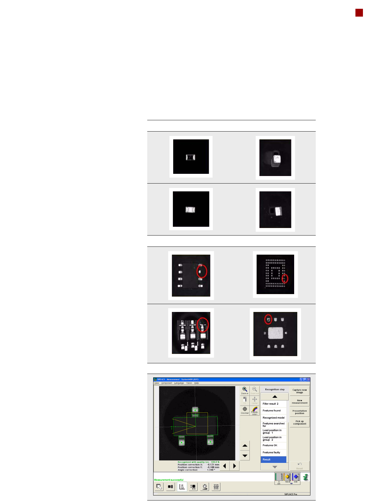
SIPLACE Vision algorithms
help with the detection of
• flipped components
• upright components
• poor component quality
The digital SIPLACE Vision
System automatically saves
the last 500 images of com-
ponents that were identified
as "bad". SIPLACE users
can then easily demonstrate
poor component quality.
The benefits at a glance:
• Maximum placement qual-
ity
• High first pass yield
• Reduced operating costs
Flipped components Upright components
Poor component quality
Vision Teach menu at the station

24
Vision Sensor Technology
PCB Position Recognition
Description
Different fiducial shapes
prove to be optimal depend-
ing on the condition of the
surface. Particularly advis-
able for bare copper surfaces
with little oxidation is the
single cross. Maximum
accuracy is achieved due to
the high information content.
Rectangle, square and circle
are less "informative" but
save space and can even be
used when oxidation is at an
advanced stage. Advisable
for tinned structures are
circle or square because in
this case the ratio of the fidu-
cial dimensions to the presol-
der thickness is particularly
favorable.
Fiducial criteria
Locate 2 fiducials
Locate 3 fiducials
X-/Y-position, rotation angle, mean PCB distortion
in addition: shear, distortion in X- and Y-direction separately
Fiducial shapes Synthetic fiducials: circle, cross, square, rectangle, rhom-
bus, circular, square, and rectangular contours, double
cross, any pattern
Fiducial surface:
copper
tin
Without oxidation and solder resist
Fiducial warp 1/10 of structure width, both with good
contrast to environment
Dimensions of synthetic fiducials
min. X/Y size for circle and rectangle: 0.25 mm
min. X/Y size for annulus and rectangle: 0.3 mm
min. X/Y size for cross: 0.3 mm
min. X/Y size for double-cross: 0.5 mm
min. X/Y size for lozenge: 0.35 mm
min. frame width for annulus and rectangle: 0.1 mm
min. bar width / bar distance for cross, double-cross: 0.1 mm
max. X/Y size for fiducial shapes: 3 mm
max. bar width for cross / double-cross: 1.5 mm
min. tolerances, general: 2% of nominal dimension
max. tolerances, general: 20% of nominal dimension
Dimensions of patterns
min. size
max. size
0.5 mm
3 mm
Fiducial environment Clearance around reference fiducial not necessary if there
is no similar fiducial structure in the search area