Brochure-PacTech-Solder-Jetting-Laser-Bonding.pdf - 第7页
Contact us at sales@pactech.com PacT ech - Packaging T echnologies GmbH Am Schlangenhorst 7 – 9, 14641 Nauen, Germany PacT ech USA Inc. 328 Martin Avenue, Santa Clara, CA 95050, USA PacT ech Asia Sdn. Bhd. No.14, Medan B…
7 8
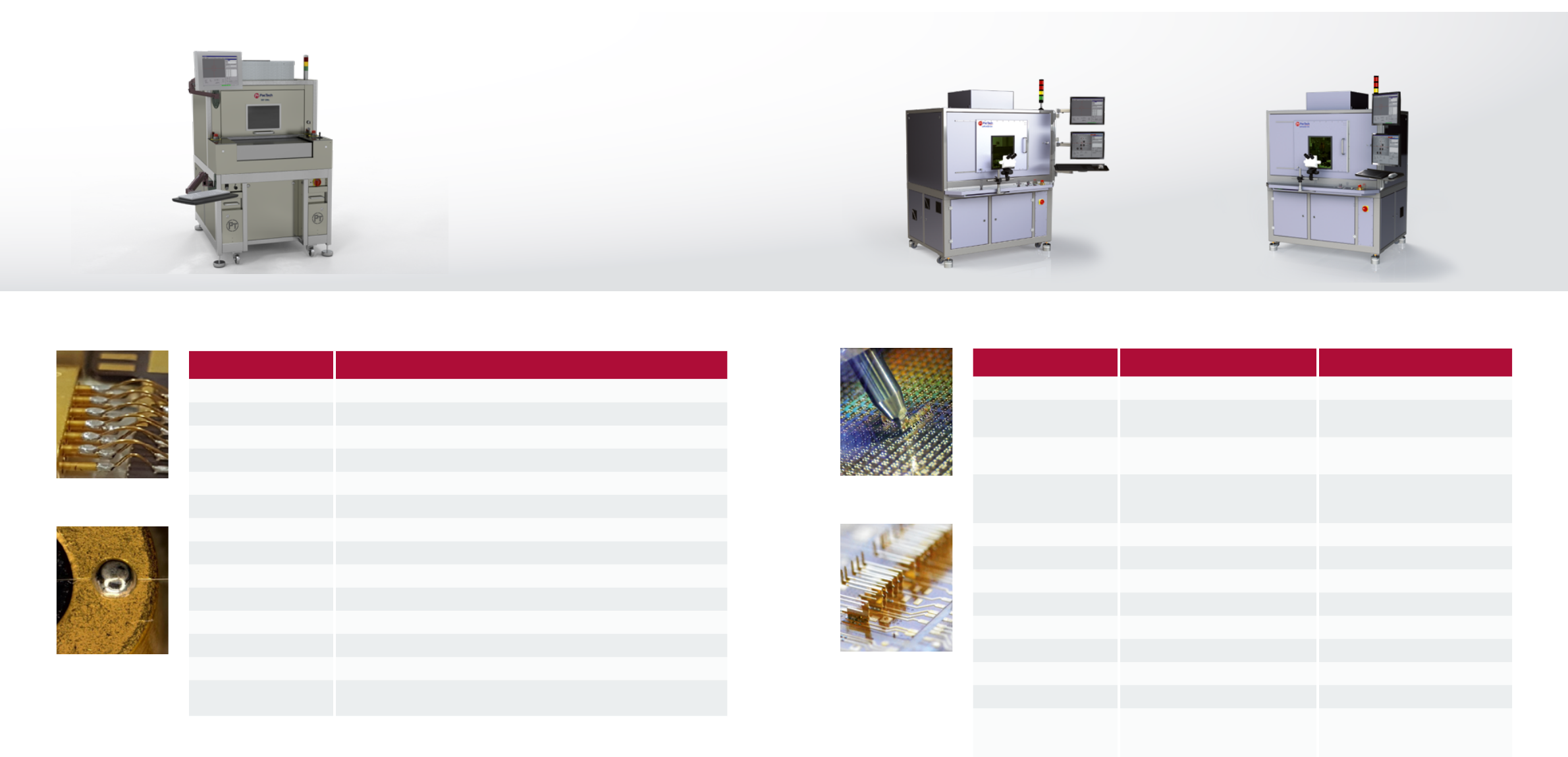
Applications
SB
2
-WB
The SB²-WB is a combination of PacTech´s unique sol-
der ball jetting technology with a wire feeding mecha-
nism to perform wiring process. This innovative solution
has very low stress as it is bonded with very short laser
pulse and requires no mechanical contact. The system is
highly exible, with various loop formation capabilities or
even no wire loop formation to enable smaller package
size, at the same time allowing combination of dierent
solder alloy and wire, wire bundles or ribbon. Higher re-
liability as compared to conventional wire bonding with
consistent wire thickness and better match of CTE varia-
tion between materials. Additionally, the solder wire bond
can be reworked selectively at ease. SB
2
-WB is a exible
wire-bonding alternative for multifunctional system plat-
forms and heterogeneous integration.
Optical bres
wiring
Connector Joining
Advanced Wire Bonding Solution
Technical Specications
Model
SB
2
-WB
SOLDER JETTING
SB² - WB
Dimension
1200 x 1300 x 1950 mm
Workspace
≥ 150 x 150 mm or 320 x 320 mm
Solder Ball Speed
2 – 4 sec per pin/pad connection
Material Ø
Solder ball Ø ≥ 50 µm; wire Ø ≥ 100 µm
Prefered Pad Material
NiAu, Au, Cu
Accuracy
+/- 5 µm (1 sigma)
Work Station
Chuck / In-line conveyor
Laser Man. Alignment
ü
Laser Auto Alignment
Optional
Pattern Recognition
ü
2D Applications
ü
3D Applications
ü
Repair
ü
Products
IC packaging, LED packaging, connectors, optical bre, 2D/3D packaging
and others
Applications
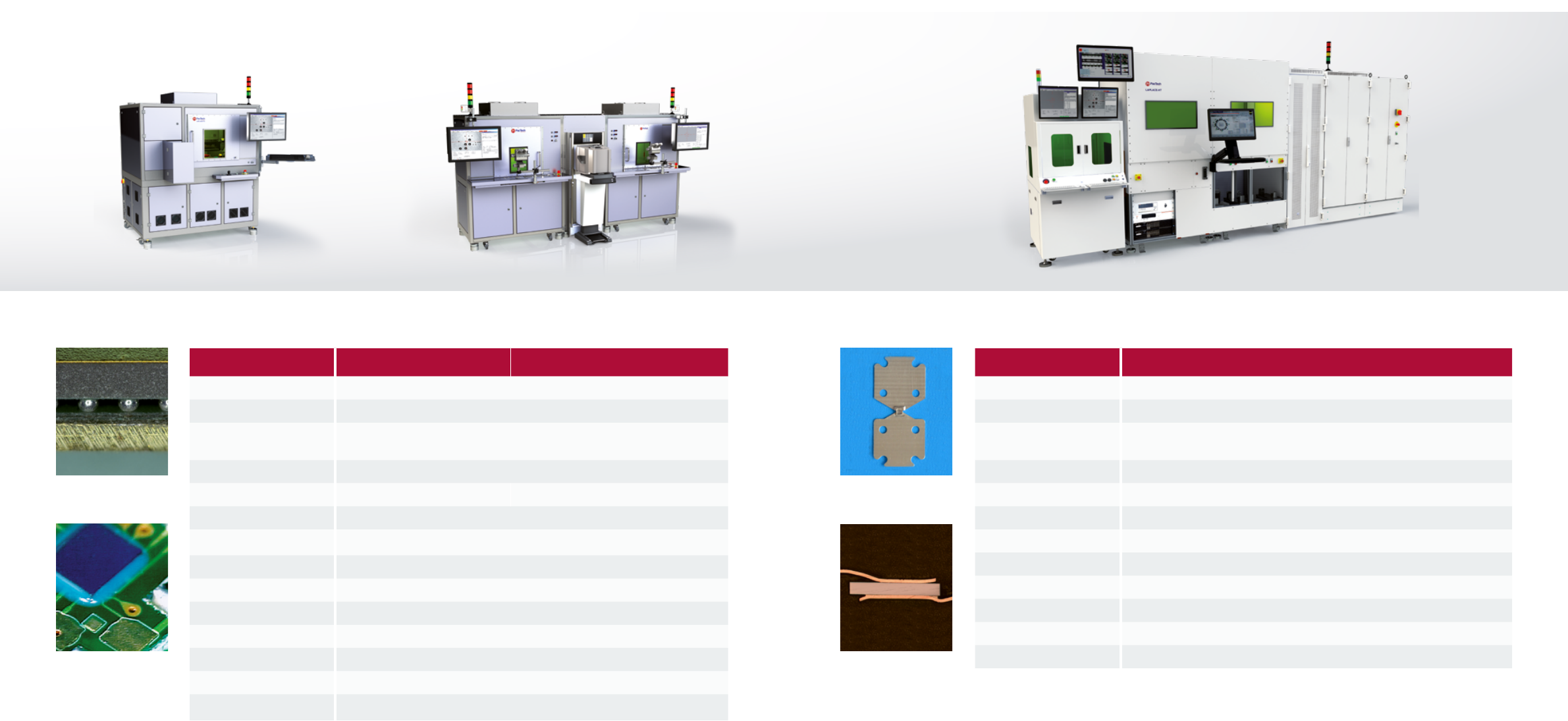
LAPLACE-Can/LAPLACE-VC
Our solution for ultra-ne-pitch cantilever assembly and
laser bonding for wafer probe cards with optional rework
capability.
This platform is also suited for the vertical attachment of
chips or similar devices loaded into the machine from feed-
ing station to various carrier substrates loaded manually
onto the machine’s work stage. The system uses a unique
patented laser thermode tool, which is integrated in the
vacuum pick and place unit of the bonder. For the high
exibility of the laser thermode, the system requires only a
thin layer of solder on the substrate.
Cantilever
Assembly
Vertical Chip
Bonding
Ultra Fine Pitch Assembly
LAPLACE-Can LAPLACE-VC
Dimension
1520 x 1100 x 1890 mm 1520 x 1100 x 1890 mm
Workspace
Work area: 330 x 330 mm
Substrate size: up to 500 x 500 mm
Work area: 330 x 330 mm
Substrate size: up to 500 x 500 mm
Cycle time
(pick & place incl. Laser reow)
≥ 7 sec / pin ≥ 10 sec / chip
Accuracy
Placement: +/- 3.5 µm (3 sigma)
Hump tilt: +/- 3 µm
Height control: +/- 4 µm
+/- 3 µm (1 sigma)
Tooling
Customized bond tool Customized bond tool
Die Handling
Wae Pack / Probe Wafer Wae Pack / Wafer
Substrate Handling
Manual / Automatic Manual / Automatic
Product Output
Manual / Automatic Manual / Automatic
Pattern Recognition
ü ü
2D Applications
– –
3D Applications
ü ü
Repair
optional –
Products
Probecards, DRAM,
ash memory, NAND
Memory chips, diode (photodiode,
LED, µLED), MEMS (sensors,
gyroscopes, etc.)
Technical Specications
Model
LAPLACE-Can
Model
LAPLACE-VC
LASER BONDING
9 10
Applications
Model
LAPLACE-FC / LAPLACE-GENESIS
LAPLACE-FC
The LAPLACE-system provides an integrated solution for
ip chip assembly, the laser reow will be done during the
placement – all in one step. The laser assisted assembly
can be applied for soldering, ACF and NCP interconnec-
tions. The optional dispensing unit in the ip chip assembly
platform allows a maximal exibility for ux, solder paste
and/or ACF, NCP dispensation.
LAPLACE-FCR:
The LAPLACE-FCR is an automatic laser bonding system
for ip chip assembly and chip rework, enabling localized
rework without second reow and mechanical pressure
to the completed units. The system will remove defect ip
chips from the wafer or carrier substrate with the vacuum
bond tool based on pre-dened mapping les or 2D in-
spection. New chips are loaded from customizable feeding
station such as wae pack prior to laser assembly.
Flip-Chip Rework
Flex to ex bonding
LAPLACE-FC LAPLACE-GENESIS
Dimension
1500 x 1200 x 2200 mm
Workspace
320 x 320 mm
Cycle time
(pick & place incl. Laser reow)
≥ 5 sec / chip
Chip size
≥ 0.3 x 0.3 x 0.1mm
Accuracy
+/- 4.5 µm (3 sigma) +/- 0,5 µm (3 Sigma)
Tooling
Customized bond tool
Die Handling
Wae Pack, Sawing Frame, Tape and Reel
Substrate Handling
Manual / Automatic
Product Output
Manual / Automatic
Pattern Recognition
ü
2D Applications
ü
3D Applications
–
Repair
optional
Products
Flip Chip, passive components, sensors, MEMS
Technical Specications
Model
LAPLACE-FCR
Flip Chip Attach & Rework
LASER BONDING
LAPLACE-HT
The LAPLACE-HT is an automatic laser soldering assem-
blyline for schottky diodes and bypass diodes – especially
for solar cell modules. Using a rotary table the automat-
ic machine punches and forms lead frames, dispenses
solder paste and performs diode laser attach to the lead
frame. A nal electrical and visual test is done on the as-
sembled modules and chip packages within the machine.
A complete standalone turnkey solution! Additional appli-
cations are LED, MOSFET and camera module assembly.
LAPLACE-HT
Dimension
5000 x 3000 x 2200 mm
Workspace
Customizable work station
Cycle time
(pick & place incl. Laser reow)
≤ 1 sec / component
Accuracy
+/- 50 µm (1 sigma)
Tooling
Customization based on product
Die Handling
Sawing Frame, Tape and Reel
Substrate Handling
Automatic
Product Output
JEDEC Tray, others
Pattern Recognition
ü
2D Applications
ü
3D Applications
ü
Products
Bypass diode for solar cells, LEDs, chips on lead frame
Bypass Diode
Cross section of
assembled Diode
Integrated Diode Assembly
Applications Technical Specications
LASER BONDING
Model
LAPLACE-HT
Disclaimer: The data provided in all technical specications are reference data from standard platforms and may vary
subject to application, modication and customization.
Contact us at sales@pactech.com
PacTech - Packaging Technologies GmbH
Am Schlangenhorst 7 – 9, 14641 Nauen, Germany
PacTech USA Inc.
328 Martin Avenue, Santa Clara, CA 95050, USA
PacTech Asia Sdn. Bhd.
No.14, Medan Bayan Lepas, Technoplex, Phase 4
Bayan Lepas Industrial Zone, 11900 Bayan Lepas,
Penang, Malaysia
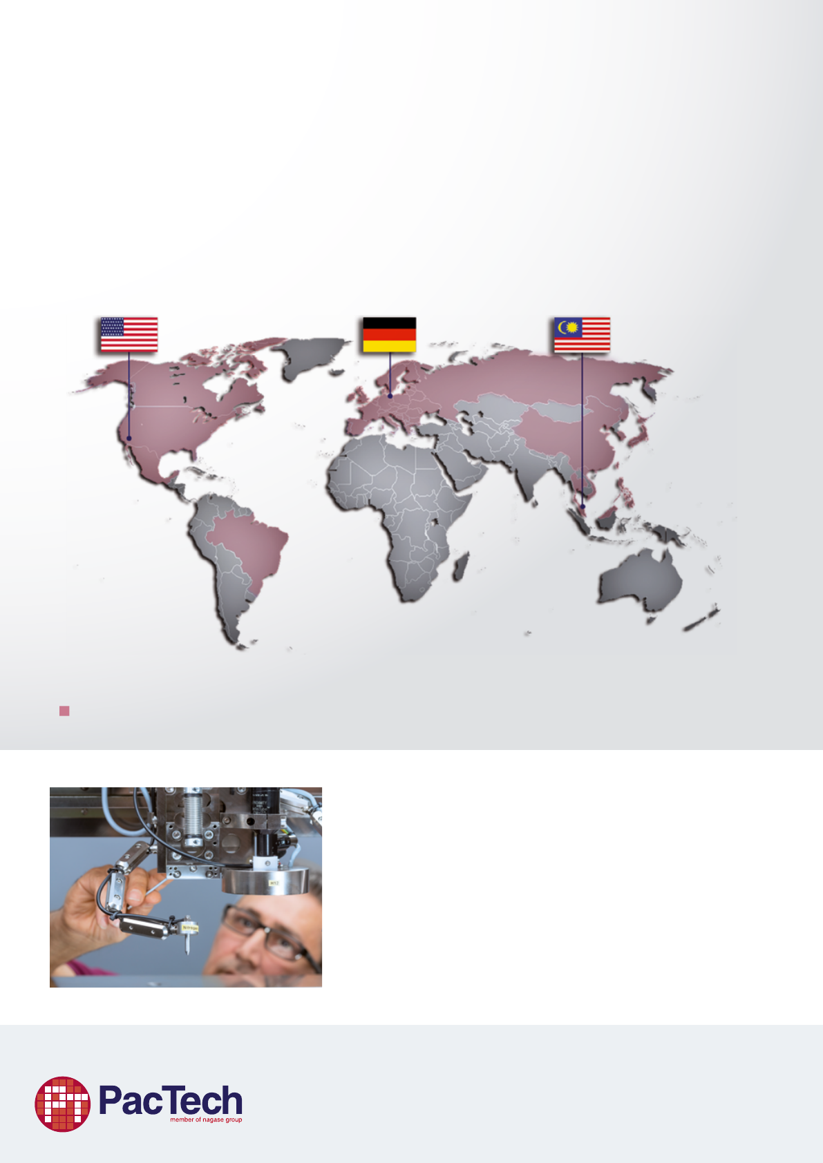
PacTech, a Global Company
Global Presence
PacTech is a wholly-owned subsidary of parent corporation NAGASE & C0., Ltd., has three operation and manufacturing
sites across three continents, covering Europe, America and Asia including the headquarters in Germany. Additionally,
PacTech has local eld service support oces for on-site technical assistance and local warehouse for immediate spare
part supply to ensure continuous operation.
Legend:
LocalFieldServiceSupportOces
PacTech USA
Santa Clara, Unites States
PacTech GmbH
Nauen, Germany
PacTech Asia
Penang, Malaysia
ISO & ITAR Certied
PacTech is ISO 9001, ISO 14001, IATF 16949 and ISO 50001
certied. Striving to deliver utmost quality to all customers, PacTech
adapts in-depth quality management system in its manufacturing
operations and every employee is dedicated to the total continuous
improvement company wide.