Anritsu机器学习应用于PCB外观检测.pdf - 第4页
Anritsu T echnical Revi ew No.28 September 2020 Application o f Machine Lear ning to Print ed Circuit Boar d External I nspection (4) This software was run on on e Image T raining PC on the AOI LAN (Figure 4). AOI-relate…
Anritsu Technical Review No.28 September 2020 Application of Machine Learning to Printed Circuit Board External Inspection
(3)
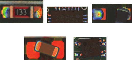
Figure 3 Examples of SMT Mounting Faults
(1) Poor wetting
The solder is not spread evenly in the correct amount over
the part leads and electrodes and the fillet form does not
appear wetted. The causes are insufficient solder, leads or
electrodes not in contact with land, and insufficient heat at
reflow.
(2) Solder bridging (shorts)
This problem tends to occur when using very small SOP
and QFP ICs with sizes of 0.5 mm and 0.4 mm
Note 4
or when
the correct amount of solder is not applied to adjacent leads.
The causes are poor solder printing, bent solder leads, and
poor parts mounting.
(3) Vertical chip (gravestone and Manhattan)
This problem occurs when both electrodes of a part are
not soldered simultaneously and surface tension at the end
wetted first causes the chip to stand vertically on one sol-
dered electrode.
The countermeasures are improving the land dimensions
and mounting accuracy, and preheating to reduce the solder
melt time difference.
(4) Non-contact, missing solder
This is caused by the solder paste not melting during re-
flow and remaining in a paste state. The causes are old
solder paste or poor reflow oven temperature control.
Missing solder is caused by lack of solder at the part and
is caused by poor solder paste printing.
(5) Rotated and slipped parts
Rotated or slipped parts are the result of part leads or
electrodes projecting outside the land or from poor posi-
tioning by the parts mounter. Vibration at mounting other
parts or at conveying/transport between processes can re-
sult in surface tension issues causing displacement as in
vertical chip faults.
Note 3: The land is a part where the copper forming the PC board
traces is exposed for soldering to the part leads and elec-
trodes. Sometimes the land surface is gold-plated.
Note 4: SOP and QFP describe IC packages. A SOP (Small Outline
Package) has L-shaped legs from two sides of the rectan-
gular package connecting to lands. A QFP (Quad Flat
Package) has multiple leads on all four sides of the package
connecting to lands.
4 AOI PC Board External Inspection Issues
AOI inspection sets strict evaluation criteria using mul-
tiple parameters so as to not allow fail products to pass in-
spection. As a result, so-called "excess watching" is a com-
mon problem. Excess watching is a phenomenon where
products passing at the visual-inspection level are evalu-
ated as fail by the AOI inspection system. If there is too
much excess watching, visual confirmation after automatic
inspection is increased.
To proactively suppress excess watching, the soldered
part digital evaluation criteria are readjusted repeatedly
over but there can be a problem where excess watching does
not decrease because fine-adjustment cannot be completed
due to momentary changes in the processing conditions
caused by PC board condition and parts mounting ran-
domness.
5 PC Board External Inspection using Machine
Learning
Applying machine learning to the visual confirmation
work following AOI inspection has helped with excess
watching inspection efficiency.
5.1 Leaned Image Data Acquisition
Collecting and annotating (labeling) images used for
machine learning is a key process in applying machine
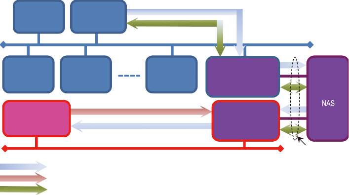
learning. Consequently, we configured a system (Figure 4)
to capture AOI inspection image data for use as learning
images.
Generally, dedicated terminals are required to capture
AOI inspection results and inspection image data. In this
development, we obtained the terminal interface specifica-
tions from the AOI maker and developed software to di-
rectly capture inspection results and learning images (in-
spection images) at a connected personal computer (PC).
(a) Poor wetting
(b) Solder Bridge
(c) Vertical Chip
(d) Missing Solder
(e) Rotated Part
47
Anritsu Technical Review No.28 September 2020 Application of Machine Learning to Printed Circuit Board External Inspection
(4)
This software was run on one Image Training PC on the
AOI LAN (Figure 4).
AOI-related PCs are connected over a dedicated AOI local
area network (LAN) from the viewpoint of higher security
and to prevent non-factory network problems affecting
plant mass-production.
To assure the independence of the AOI LAN, the ma-
chine-learning environment ( and in Figure 4) was con-
figured on the in-company LAN via a separate independent
LAN (c. Independent LAN in Figure 4) and multiport Net-
work Attached Storage (NAS) ( in Figure 4).
Required data is shared via files on the NAS and the PC
for capturing learning images is programed to send images
and evaluation data stored on the AOI-DB server periodi-
cally to the machine-learning PC.
Generally, at machine learning, only images of pass
products are required, but not images of faulty products.
However, due to disk-space limitations at the AOI-DB serv-
er, there were problems with inability to save images for
products evaluated as pass. Consequently, the focus of at-
tention was only on trouble locations such as electrodes and
leads for images of parts evaluated as fail and machine
learning was used to capture images of fillets of electrodes
and leads of pass parts from within images of fail parts.
When introducing machine evaluation to external inspec-
tion, the learning model obtained from the Ma-
chine-Learning PC was transferred to the Machine Evalua-
tion PC and the result for the evaluated image was saved in
the AOI-DB server as the visual evaluation result that the
Image Training PC input to the AOI terminal. If images
evaluated by AIO as fail were evaluated by machine learn-
ing as pass, the operator in charge of visual evaluation
handled the image as if it had already been visually evalu-
ated.
Reduction of visual inspection and confirmation by eye is
expected with introduction of machine learning because
only parts evaluated as fail by both AOI and machine
learning are inspected.
5.2 Machine Learning Discriminator
Machine learning is a method for allowing a computer to
learn human-like recognition and evaluation. It is per-
formed using the following two processes: Learning, and
Evaluation
1), 2), 3)
.
(1) Learning Process
Even the best machine-learning algorithm is worthless
without a learning process which must be performed first
using learning data. Learning is repeated over until the
accuracy (learning mistakes) reach the required accuracy
and the learning model is completed.
(2) Evaluation Process
The discriminator (model with completed learning) eval-
uates whether input image data are pass or fail. For exam-
ple, a discriminator that has learned labelled (named)
product images can accurately evaluate the names of prod-
ucts for unknown images that have not been learned.
a. AOI LAN
b. Company LAN
(1) Training image and AOI evaluation result
(2)
Evaluation m
achine learning model
(3) Board evaluation image and result (at machine evaluation introduction)
(1)
(2)
(3)
(1)
c. Inde
p
endent LAN
Image
Training PC
(Windows10)
AOI-DB
Server
AOI
Main
AOI
Terminal
AOI
Terminal
AOI
Terminal
Machine
Learning PC
(Linux)
Machine
Evaluation
PC (Linux)
Figure
4
Image Acquisition System Configuration
48
Anritsu Technical Review No.28 September 2020 Application of Machine Learning to Printed Circuit Board External Inspection
(5)
(3) Discrimination Procedure
We used a convolutional neural network with excellent
image-recognition performance as the machine-learning
discriminator. A convolutional neural network is configured
from a pile of levels, such as convolution layers and pooling
layers with various special functions to form a number of
deep levels. The convolutional neural netwok used in this
study had 10 levels composed of convoluted layers with co-
efficients of 3 × 3 and 3 × 1 (height × width).
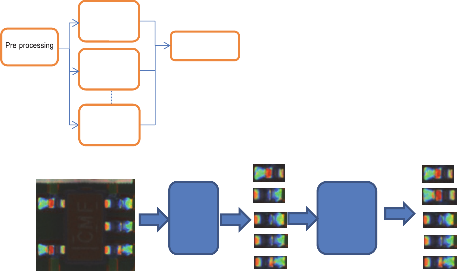
Figure 5 illustrates the discrimination procedure. First,
pre-processing loads the image to be inspected and identi-
fies the solder locations. The solder locations identified by
the discriminator are output as numeric discrimination re-
sults in the range of 0.0 to 1.0 indicating the normality dis-
tribution of the solder locations, with a value of 1.0 being
maximum normality. The normality threshold value deter-
mines whether the solder joint condition is pass or fail.
As shown in Figure 6, this inspection uses multiple dis-
criminators and evaluation is performed using the model
average, which averages the output of each discriminator.
Better performance can be expected
1), 2)
with suppressed
randomness, etc., by changing the learning parameter de-
fault values and combining multiple discriminators than
when using a single discriminator.
Figure 6 Model Averaging
6 Evaluating Results of PC Board External In-
spection using Machine Learning
6.1 Detection Performance
The performance of the algorithm proposed in this article
was evaluated using the model averaging technique applied
to 560 inspection images of pre-specified parts (60 pass
parts and 500 fail parts). The images used for evaluation
were not used for learning.
The results are shown in Table 1; eight learning models
were provided. As shown in Table 1, model averaging was
performed without making a specific evaluation to suppress
randomness in the detection performance for each learning
model.
Figure 7 shows the cumulative distribution confirming
the normality distribution. The red line is the cumulative
distribution of normality for fail parts (493 locations) and
the blue line is the cumulative distribution of normality for
pass parts (65,168 locations). The fail parts cumulative dis-
tribution origin is 1.0, but is best if distributed in the lower
half with the origin at less than 0.5. In addition, the pass
parts cumulative distribution is the distribution with 0.0 as
the origin, but is best if distributed in the upper half with
the origin at more than 0.5. Since the cumulative distribu-
tions for the pass and fail locations intersect, evaluation
mistakes occur when evaluating using a threshold.
Machine
Learning
Discriminator 1
Machine
Learning
Discriminator 2
Model Average
Machine
Learning
Discriminator N
Machine
Learning
Discriminator
Inspection
Image
(Input Image)
Extraction of Slder
Joints at 5 Locations
Discrimination
Processing for Each
Location
Normality of Each
Joint
Pre-
processing
0.2
0.3
0.8
0.9
1.0
Figure 5 Discrimination Procedure using Machine Learning
49