ED-7306_E.pdf - 第17页
JEITA ED-7306 - 15 - Explanatory Table 1 Maximum permissi ble package warpage for BGA and FBG A Unit: mm Solder ball pitch 0.4 0.5 0.65 0.8 1.0 1.27 Condition of solder ball height a) 0.20 0.25 0.33 0.35 0.40 0.50 0.60 C…
JEITA ED-7306
- 14 -
3.5 Maximum permissible package warpage of BGA and FBGA
3.5.1 The maximum permissible package warpage of BGA and FBGA is described in Explanatory Table 1,
which is calculated from the experimental data.
3.5.2 Given that PWB is an ideally flat seating plane, the maximum relative displacement from the seating
plane is the difference between the highest and lowest joint heights of BGA which is immune from the
open solder joints or solder ball bridges.
3.5.3 The maximum permissible package warpage of BGA and FBGA is determined to be 80 % of the
maximum relative displacement, where either open solder joints or solder ball bridges was not seen.
The other 20 % is given to the permissible warpage of PWB. The ratio reflects the difficultness in
maintaining straight of the package versus PWB at elevated temperature, i.e. complexity in the
materials and structure of package vs. PWB.
3.5.4 The criteria of maximum permissible package warpage for solder joints without open or short circuits
are obtained separately. Less than 10 µm of difference indicate that the open solder joints and solder
bridges are the phenomena caused by the same reason but viewed from opposite sides. The current
magnitudes of package warpage barely satisfy the budget allocation of the tolerance, 80 % to the
package. However, along with the progress in technology, the methodology to reduce the package
warpage will be established, and then the criteria will be reviewed.
JEITA ED-7306
- 15 -
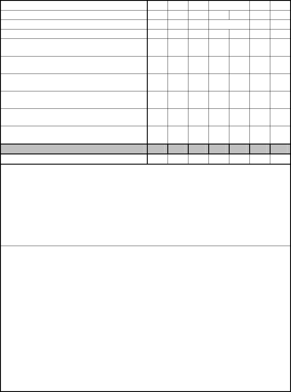
Explanatory Table 1 Maximum permissible package warpage for BGA and FBGA
Unit: mm
Solder ball pitch 0.4 0.5 0.65 0.8 1.0 1.27
Condition of solder ball height
a)
0.20 0.25 0.33 0.35 0.40 0.50 0.60
Condition of solder paste thickness after reflow
b)
0.08 0.10 0.11 0.13 0.14 0.15
Nominal solder joint height of the ideally flat package 0.18 0.23 0.29 0.31 0.36 0.43 0.5
Highest solder joint height of BGA without open
solder joint
c)
0.28 0.35 0.44 0.48 0.53 0.64 0.75
Lowest solder joint height of BGA without open
solder joint
d)
0.16 0.20 0.25 0.27 0.31 0.37 0.44
Highest solder joint height of BGA without solder
bridge
e)
0.24 0.29 0.38 0.40 0.46 0.55 0.66
Lowest solder joint height of BGA without solder
bridge
f)
0.12 0.15 0.20 0.19 0.25 0.28 0.34
Max relative displacement of BGA without open
solder joint
g)
0.12 0.15 0.19 0.21 0.22 0.27 0.31
Max relative displacement of BGA without solder
bridge
h)
0.12 0.14 0.18 0.21 0.21 0.28 0.32
Max permissible package warpage (Absolute value)
i)
0.10 0.11 0.14 0.17 0.17 0.22 0.25
Coplanarity at room temperature (For reference) 0.08 0.08 0.10 0.10 0.10 0.20 0.20
NOTE: Assumptions of the calculations are
• The structure of the lands on PWB is non solder mask defined;
• The diameter of the lands on PWB is the same as that of package;
• Solder joint height between package and PWB is the distance between the face-to-face copper
lands;
• Thicknesses of the metal masks for solder paste printings are
- 0.10 mm for 0.4 mm pitch FBGA,
- 0.12 mm for 0.5 mm and 0.65 mm pitch FBGA, and
- 0.15 mm for 0.8 mm, 1.0 mm, and 1.27 mm pitch BGA;
• Opening diameter of the solder printing mask is the same as that of the lands on PWB.
Table footnote:
a)
It follows the specification in JEITA EDR-7315 and JEITA EDR-7316.
b)
It is the thicknesses of molten solder paste on copper lands without any component attached,
supposed 50 % of solder paste is metal content (solder).
c)
It is the sum of the solder ball height and the molten solder-paste thickness, where the solder
connections are immune from open circuit.
d)
It is 87 % of the nominal standoff height of the ideally flat package. The ratio is obtained from the
empirical data taken from the intentionally concave-warped sample.
e)
It is 130 % of the nominal standoff height of the ideally flat package. The ratio is obtained from the
empirical data taken from the intentionally convex-warped sample.
f)
It is the sum of the molten solder and the solder ball height when the ball diameter expands to 80 % of
the ball pitch. It is known that the balls do not bridge as far as the collapse of solder balls does not
make the ball diameter expand beyond 80 % of the ball pitch.
g)
It is the difference between the highest and the lowest solder joint height, where open solder joint is
not seen.
h)
It is the difference between the highest and the lowest solder joint height, where solder ball bridge is
not seen.
i)
It is 80 % of the maximum relative displacement.
JEITA ED-7306
- 16 -
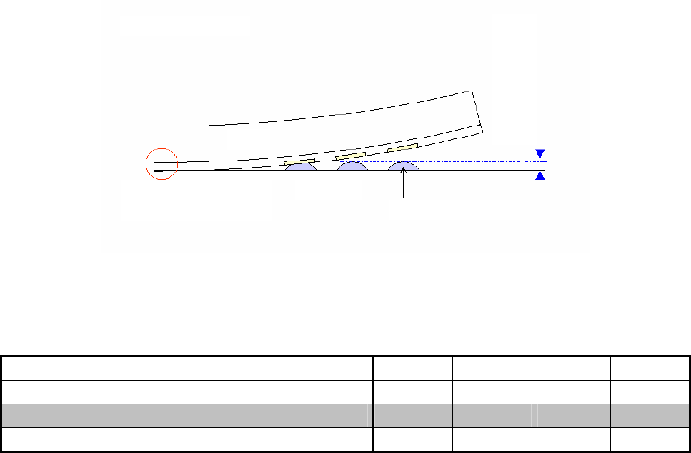
3.6 Maximum permissible package warpage of FLGA
Given that PWB is an ideal seating plane, the maximum package warpage is defined to be the thickness of
molten solder paste. (See Explanatory Fig. 3) However the maximum permissible package warpage
depends on the amount of the solder paste, the criteria for FLGA are specified in Explanatory Table 2 for
semiconductor suppliers.
Explanatory Fig. 3 Package warpage of FLGA at elevated temperatu
Explanatory Table 2 Maximum permissible package warpage for FLGA
Unit: mm
Land pitch 0.4 0.5 0.65 0.8
Condition of thickness of molten solder 0.08 0.10 0.11 0.13
Maximum permissible package warpage (Absolute value) 0.08 0.10 0.11 0.13
Coplanarity at room temperature (For reference) 0.08 0.08 0.10 0.10
3.7 Discussion with the TSC on Jisso Technology Standardization
After drafting this specification, the task force requested the TSC on Jisso Technology Standardization to
review this specification and to hold the joint ad hoc meeting to promote harmonization of the opinions
between suppliers and users. Most of the issues raised by TSC were corrected or added, but there were
some disagreements left. Chief request was to verify if the measurement data from different types of
instruments are well accorded with. With the collaboration of measuring instrument suppliers, the bimetal
samples were measured by 3 types of instruments.
Since the TSC on Jisso Technology Standardization did not have enough data to comment on the criteria of
the maximum permissible package warpages, they would review the criteria one year later after the
collection of the data of the package warpages and the board assembly yields.
4. Industry property rights
The task force surveyed the industrial property rights that directly related to the measurement methods and
the maximum permissible warpage but did not find any of them.
FLGA
Maximum permissible
package warpage at
elevated temperature
Molten solder paste
PWB
The lowest point where
FLGA settles on PWB.
FLGA warpage