Tech Article._X-ray Inspection_Final Version.pdf - 第4页
early stages is also gener ally easier . For ex ample, nding void de f ec ts in waf e r bumps (g. 4 ) bef ore an y other lay e r s have been added, comp are d to a fully f ormed chiple t consisng of mulple devices, s…
The complete inspecon picture
Nordson TEST & INSPECTION designs, develops and manufactures various dierenated
technologies which complement each other: these include Acousc, Opcal and Manual X-ray
Inspecon, Autonomous X-ray Inspecon, X-ray Component Counng, Semiconductor Wafer
Metrology, Semiconductor Metrology Sensors and Nordson X-ray Technologies.
A good example is to use both acousc and X-ray inspecon. Acousc inspecon is very
strong when viewing delaminaon in the silicon wafers themselves, where this is much more
of a challenge for X-ray. If this defect is not viewed from the correct angle the imaging isn’t
able to create a clear contrast between that empty space and the material around it. But
when the sound wave in acousc imaging hits this air gap it cannot pass through, is reected
back and detected giving the strongest signal possible. Conversely, where it is dicult to get
this acousc signal back or detect it transmissively (due to scaering or obstrucon by
another void), X-ray makes inspecon simple.
In a similar way, 2D X-ray imaging is complimented by 3D inspecon allowing users to analyse
in ever greater detail.
This is done using Computed Tomography (or CT) which provides the ability to create 3D
models which can then be virtually dissected over and over again, without the need to
destroy the sample under test. This does require more images to be taken in the rst place
and therefore more me than a single 2D strategy. With the ever present need to improve
cycle mes in producon, oen referred to as units per hour (UPH), 3D may never completely
replace 2D. But the major payo is being able to isolate individual layers of devices,
exponenally increasing the chance of nding any problem areas. Something that can be
really challenging, somemes impossible when inspecng highly complex devices with 2D
imaging.
Each of these dierent perspecves have their own strengths and weaknesses. Combined,
they provide a really strong strategy, revealing any defects. Ulmately, by ulizing mulple
technologies and techniques, a more complete inspecon picture can be built up and deeper
understanding can be gained.
Today’s challenge: 3D stacking and heterogeneous ipchips
One of the hot topics in semiconductor engineering right now is 3D design. While this is being
tackled in a few forms, the need to go 3D is simple – the reducon of distance and with that,
resistance/temperature. This is one of the main factors driving the density (in terms of
number of connecons in a given space) of devices and with that the challenges in inspecon.
Given that, high resoluon imaging is clearly required as well as mulple techniques and
technologies. So is the need to implement these at dierent stages of the design and
producon process (g 3.).
We have already established this also makes sense in terms of the cost of failure by capturing
the defects early, before you have invested too much. It also follows that inspecon at the
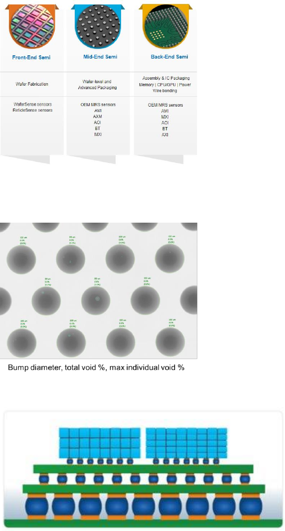
early stages is also generally easier. For example, nding void defects in wafer bumps (g. 4)
before any other layers have been added, compared to a fully formed chiplet consisng of
mulple devices, substrates and interconnecon layers (g. 5). This works out well, simple
inspecon can be done with faster, more cost eecve 2D imaging and then each of these
elements are combined when proven good. At the same me, the quality of how these have
been put together can then be inspected with the faster 3D techniques. When any of these
devices are then found to have failed, more me can be jused to gain more detail and this
insight can be fed back to improve process or design.
Fig 3. Inspecon Stages
Fig 4. 100µm bump inspecon
Fig 5. 3D Integrated Die Stack