C371347_139780418F8DFE40697A24CD62AD2CE5.pdf - 第9页
CM108B USB Audio Single C hip Datasheet Revision: 1.11 www .cmedia.com.tw P age 9 / 24 Copyright© C -Media Elect ronics Inc. 5 Bl ock diagra m Regulator 5->3.6, 3.3 & 1.8 USB Interface USB TRX EEPROM Interface RF …
CM108B
USB Audio Single Chip
Datasheet Revision: 1.11 www.cmedia.com.tw
Page 8 / 24 Copyright© C-Media Electronics Inc.
38
MSEL
DI, ST, PU
Mixer enable select:
H: push up to 3.3V, L: push down to ground
H: with mixer/AA-path enabled (with default mute)
L: without mixer/AA-path disabled
USB descriptors will also be changed accordingly
39
VOLUP
DI, ST, PU
Volume up (edge trigger with de-bouncing)
40
PDSW
DO, 4mA , OD
Power down switch control signal (for PMOS polarity)
0: normal operation
1: power down mode (suspend mode)
41
USBDP
AIO
USB Data D+
42
USBDM
AIO
USB Data D-
43
GPIO1
DIO, 8mA, PD, 5VT
GPIO pin
44
SDOUT
DO, 2mA, SR
DAC I2S data output
45
DAMCLK
DO, 2mA, SR
11.2896 MHz output for 44.1KHz sampled data and
12.288 MHz output for 48KHz sampled data
46
DALRCK
DO, 2mA, SR
DAC I2S left/right clock
47
DASCLK
DO, 2mA, SR
DAC I2S serial clock
48
VOLDN
DI, ST, PU
Volume down (edge trigger with de-bouncing)
NoteU: DI / DO / DIO – Digital Input / Output / Bi-Directional Pad
AI / AO / AIO – Analog Input / Output / Bi-Directional Pad
SR – Slew Rate Control
ST – Schmitt Trigger
PD / PU – Pull Down / Pull Up
5VT – 5 Volt Tolerant (3.3V Pad)
OD – Open Drain
P – Power Supply Pin
CM108B
USB Audio Single Chip
Datasheet Revision: 1.11 www.cmedia.com.tw
Page 9 / 24 Copyright© C-Media Electronics Inc.
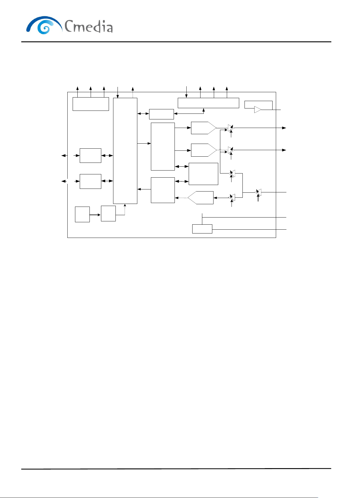
5 Block diagram
Regulator
5->3.6, 3.3 & 1.8
USB
Interface
USB TRX
EEPROM
Interface
RF
PLL
ISO Out
Processing
ISO In
Processing
12M
48M
SPI
USB
DW
DR
SK
CS
USBDP
USBDN
16 bit
DAC
16 bit
DAC
12dB/22dB
Booster
23 ~ -22dB
8 ~ -22dB
0 ~ -45dB
0 ~ -45dB
SRAM
bandgap
VREF
(1.75V)
VREF
VBIAS
(3V)
USB Control
Interface Logics
AREG36
VOLUP
VOLDN
MUTER
MUTEP
LEDO
LEDR
PWRSEL
MODE
MSEL
PDSW
3.6V
LOR
LOL
MICI
N
DREG33
3.3V 1.8V
VREF
LOBS
16 bit
ADC
DREG18
GPIOs
DASCLK/ADSCLK
DALRCK/ADLRCK
DAMCLK/ADMCLK
SDOUT/SDIN
I2S Out/In
CM108B Block Diagram
CM108B
USB Audio Single Chip
Datasheet Revision: 1.11 www.cmedia.com.tw
Page 10 / 24 Copyright© C-Media Electronics Inc.
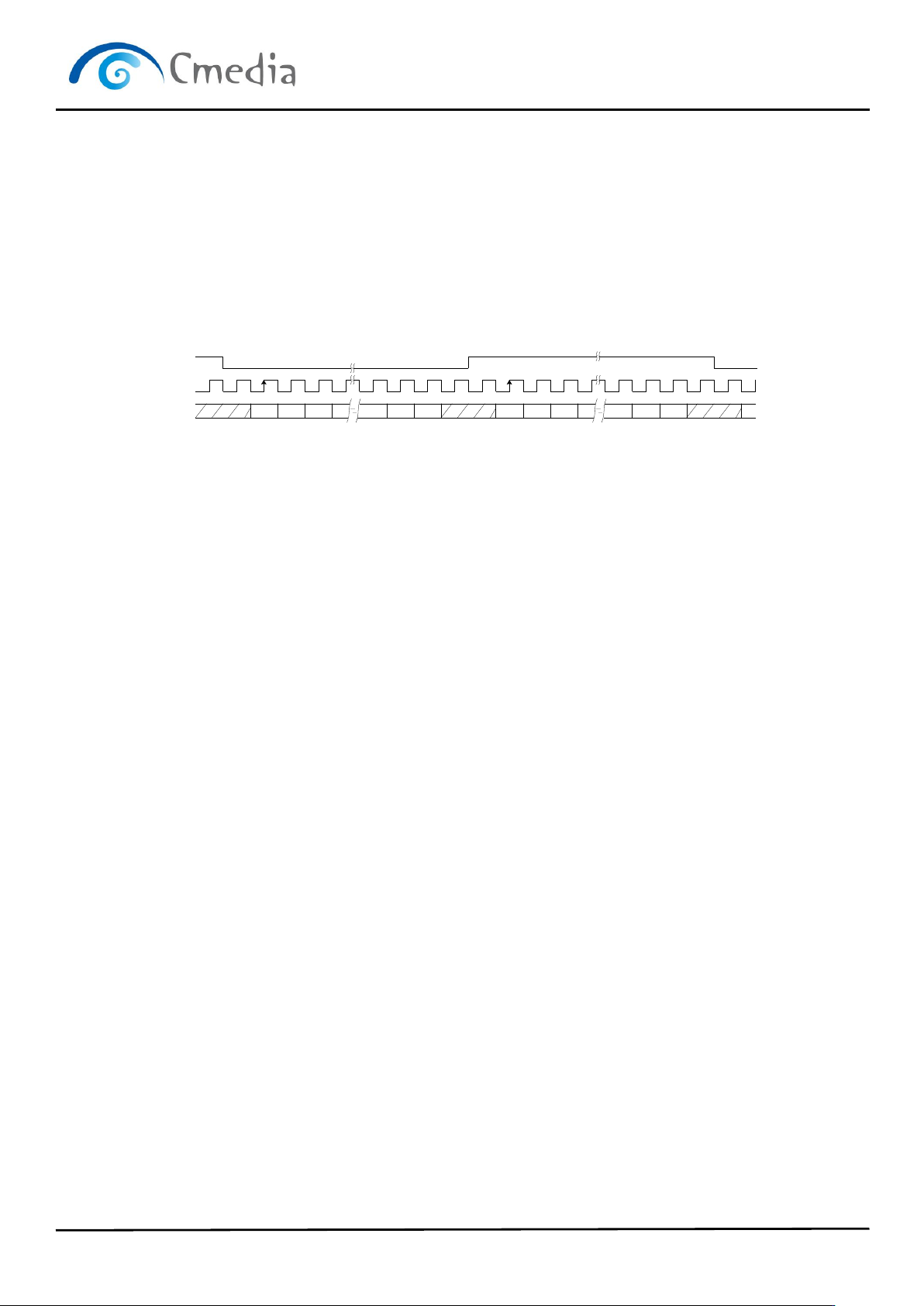
6 I2S Interface
The CM108B provides an I2S interface for both playback and recording. External ADC, DAC, or DSP can be added to
provide additional functions within the USB audio system. The CM108B sends out master clock (fixed at x256), LRCK
(fixed at x64), and data clock data. Therefore, external ADCs, DACs, or DSPs should be set to slave mode.
The left channel of the CM108B’s I2S bus is used for mono recording. Both IP
2P
S buses use a 5V tolerant pad in order
to easily interface with 5V or 3.3V devices. Playback data is simultaneously sent to both the DAC and I2S bus. The
recording source (ADC or I2S bus) can be selected by ADSEL jumper pin.
LRCK
SCLK
MSB -1 -2 +2 +1 LSB MSB -1 -2 +2 +1 LSB
SDATA
Left Channel
Right Channel