XM8000 Series Brochure EN.pdf - 第4页
6 | Nordson XM8000 Series Nordson XM8000 Series | 7 Intellig ent defec t measurement The Nordson XM8000’ s intelligenc e provides optimum defect analysis, which elimina tes the need for oper at or interpret ation and min…
4 | Nordson XM8000 Series Nordson XM8000 Series | 5
XXXXXXXX
XXXXXXXXXXXXX
XXXXXXXX
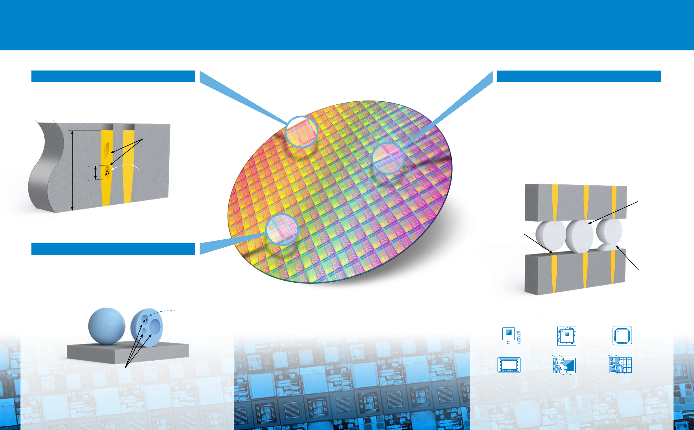
TSV Metrology
Wafer Level Packaging
Nordson XM8000-5 measures wafer bump characterization
including voiding, presence, position, shape, size and
bridging. Unlike optical tools, XM8000-5 can measure voids
within the wafer bump.
Nordson XM8000 enables in depth analysis of all forms
of wafer level packaging. This analysis is customized for
such defects such as Cold Joints, Head in Pillow (HiP),
misalignment and missing features.
The intelligent, self learning capability of XM8000 allows
unrivaled detection of micro defects in
complex packages.
Nordson XM8000-7 delivers high throughput metrology of
TSVs. Advanced 3D techniques are used to analyze shape,
fill and voiding at sub-micron levels.
Wafer Bump Metrology
Misaligned
Cold Joint
MEMS
CIS
FPGA
Memory
RF
Photonic
Head in Pillow
Void Count
Silicon substrate
Position
Position
Presence
Profile
Position
Percentage Voiding
Layer Alignment
Fill
Size
Count, Volume
Silicon substrate
Silicon substrate
TSV
Measured Solutions
6 | Nordson XM8000 Series Nordson XM8000 Series | 7
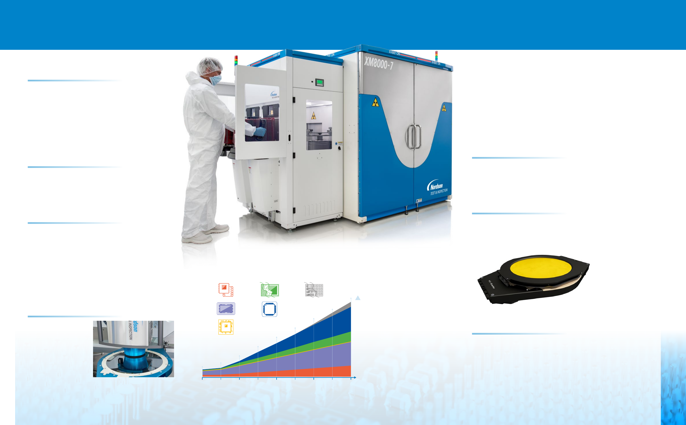
Intelligent defect measurement
The Nordson XM8000’s intelligence provides optimum
defect analysis, which eliminates the need for
operator interpretation and minimizes false calls.
As a fully automated system, exact measurement
criteria are measured, reproduced and repeatable for
consistent analysis across multiple sites, customized
to the specific device.
Continuous learning
The Nordson XM8000 continuously learns so it
can improve reliability and repeatability of defect
recognition, further eliminating false calls.
Unbeatable resolution
100nm defect recognition opens up a whole
new world of X-ray metrology applications.
The patented NT100M X-ray tube, unique to Nordson
TEST & INSPECTION, is 10 times brighter and
intrinsically more stable than conventional X-ray
tubes. NT100M utilizes a LaB
6
emitter instead of
the traditional tungsten filament, which typically only
achieves 350nm defect recognition.
Consistency as standard
With unrivaled GR&R
to less than 5%,
the XM8000 utilizes
the latest high
resolution stages
to 1um accuracy
providing supreme
repeatability.
Clean by design
The Nordson XM8000 creates an ISO3 (at rest) and ISO4 (in
motion) environment for your sample. Manufactured in a
certified clean room environment and specifically designed
for use in a semiconductor FAB, the XM8000 design has been
optimized to keep your samples clean.
Device ProtectionIntelligent Defect Analysis
As devices become more complex and sensitive
to radiation exposure, providing protection is
ever more paramount. IC-Safe Technology,
unique to Nordson TEST & INSPECTION, allows
products to be safely inspected in-line without
risk of radiation damage.
IC-Safe filters
Protect samples from X-ray over exposure with IC-Safe filters.
Specifically designed for your application to give total peace of
mind for your devices.
IC-Safe shields
When selective sampling is utilized, IC-Safe shields completely
eliminate radiation exposure to all other device samples not
under test.
IC-Safe Radiation Shield
202120202019201820172016
WLP GROWTH
2015
20142013
RF
MEMS
XXXXXXXX
CIS
XXXXXXXXXXXXX
XXXXXXXX
FPGA
Memory Photonic
RF
MEMS
CIS
FPGA
Memory
Photonic
TSV wafer starts, breakdown by application. Source:
Yole Dévelopment September 2016.
The semiconductor
market demands
increasingly complex
devices that are enabled
by technologies such
as TSV, PoP, 2.5D and
3D integration. These
complex products
demand a new level
of metrology. The
XM8000 system delivers
fully automated, non-
destructive, radiation
safe defect detection for
all complex devices.
8 | Nordson XM8000 Series Nordson XM8000 Series | 9
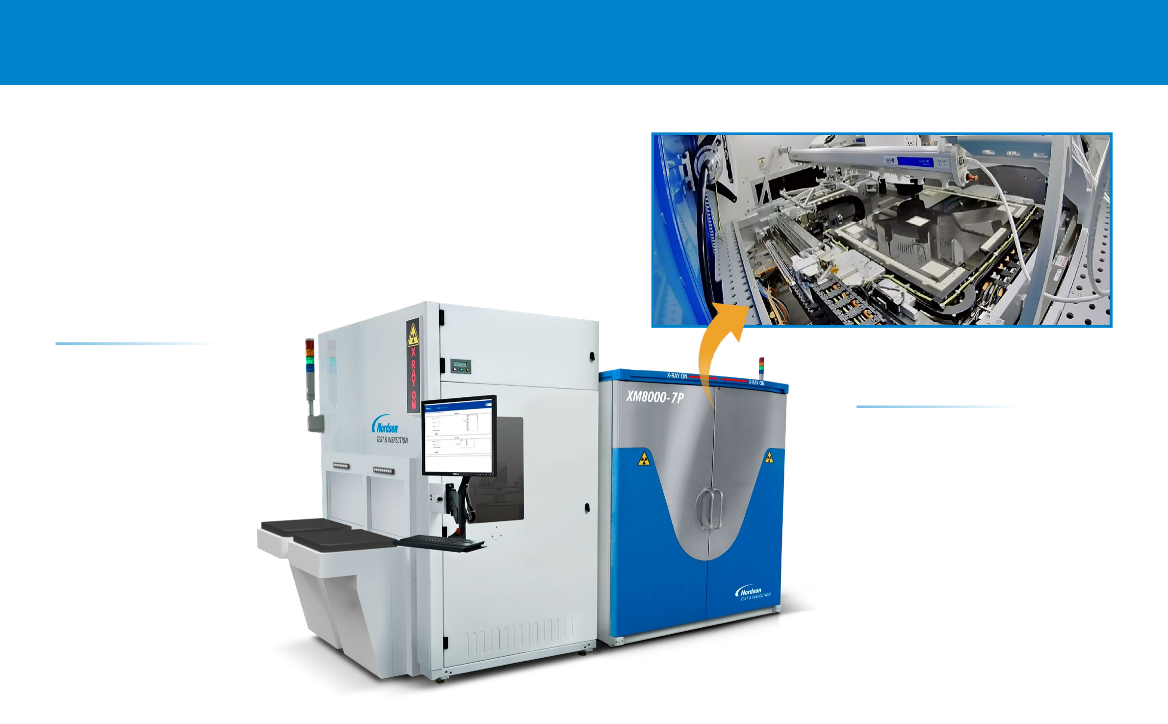
Panel Level Packages
The Nordson XM8000-7P is specifically designed for X-ray inspection
of panel level packages with maximum panel size of 510mm x 515mm.
Enabling manufacturers to identify even the smallest defects, buried
inside multi-layer semiconductor panel level packages.
The 7-axis system includes a detector gimbal for 3D
capabilities which is the pinnacle of accuracy for
fully-automated X-ray metrology.
Upgraded Handling
The XM8000-7P and EFEM has been upgraded
to support wafer panels up to 510mm x
515mm in size. The system is designed to be
tolerant to 6mm panel warpage and weights
up to 3kg.
Imaging Performance
The XM8000-7P has the same X-ray imaging chain
as the regular 7 variant. This means there is no
compromise on image quality, delivering the same
levels of accuracy and precision. High resolution
3D imaging as standard down to 0.2 micrometers
per pixel.