67021-ultraviolet-led-multi-chip-module-based-on-ceramic-substrate.pdf
Ultraviolet LED Mu lti-Chip Module Ba sed on Ceram ic Substrate Burkhardt, T. 1,2 , Hornaff, M. 1 , Acker, A. 1 , Peschel, T. 1 , Beckert, E. 1 , Suphan, K.-H. 3 , Mensel, K. 4 , Jirak, S. 4 , Eberha rdt, R. 1 , Tünnerma…
Ultraviolet LED Multi-Chip Module Based on Ceramic Substrate
Burkhardt, T.
1,2
, Hornaff, M.
1
, Acker, A.
1
, Peschel, T.
1
, Beckert, E.
1
, Suphan, K.-H.
3
,
Mensel, K.
4
, Jirak, S.
4
, Eberhardt, R.
1
, Tünnermann, A.
1,2
1
Fraunhofer Institute for Applied Optics and Precision Engineering IOF, Albert-Einstein-
Str. 7, 07745 Jena, Germany
2
Institute of Applied Physics, Abbe School of Photonics, Friedrich-Schiller-University Jena,
Albert-Einstein-Str. 15, 07745 Jena, Germany
3
Micro-Hybrid Electronic GmbH, Heinrich-Hertz-Str. 8, 07629 Hermsdorf, Germany
4
Lastronics GmbH, Winzerlaer Str. 2, 07745 Jena, Germany
*Phone: +493641807339, E-mail: Thomas.Burkhardt@iof.fraunhofer.de
Abstract
A high power ultraviolet (UV) light emitting diode (LED) multi-chip module package based on aluminum
nitride (AlN) and alumina (Al
2
O
3
) is presented. The AlN substrate with a high thermal conductivity of up to
180 W/(m·K) and LED chips based on a copper alloy provide superb thermal management and heat extraction.
Efficient cooling is an important prerequisite for the increase of extractable optical power and decrease of ther-
mally induced wavelength shift. A design of a stackable module featuring arrays of 7×2 indium-gallium-alumi-
num-nitride UV LED chips at 395 nm is developed. This configuration of sub-modules allows for the scalable
assembly of line sources with different lengths. Applications using UV LEDs cover market segments such as
curing of adhesives, inks and coatings, sterilization of medical equipment and treatment of potable water, as well
as various uses in chemical detection, biochemical analytics and spectroscopy.
Thermal and thermo-mechanical modelling of the sub-mount is conducted using finite elements analysis. Die
attach using eutectic gold-tin solder, lower melting tin-lead solder and silver-filled adhesive are compared with
respect to optical output power and wavelength drift. Mechanical strength and structure of the resulting joints are
investigated using shear force measurements, cross-sectioning and micro-tomography. An optical output power
of 7.7 W is achieved using a cluster of 14 LED chips at 1050 mA resulting in a peak irradiance of 30.8 W/cm² at
the LED surface with respect to the footprint and pitch of the attached chips.
Key words: solid state lighting, ceramic packaging, ultraviolet light emitting diode, ceramics
Introduction
UV-sources are used in a wide field of applications
such as the curing of adhesives, inks, coatings and
industrial paints, the sterilization of medical equip-
ment and the treatment of potable water. Further-
more such light sources are needed for a various
uses in chemical detection, biochemical analytics
and spectroscopy. Currently high power mercury
gas-discharge lamps are used to cover this wave-
length range. Due to the high temperature of the
discharge tubes and the infrared (IR) radiation
characteristics such lamps find limited use in the
processing of temperature sensitive materials, e. g.
the curing of paints on plastics. Solid state light
sources based on UV-LED however offer a solution
for the abandonment of toxic mercury lamps, while
providing additional benefits as smaller form factor,
increased lifetime and ruggedness, an application
tailored emission spectrum with reduced IR
emission and added flexibility to UV applications
[1], [2]. High power density UV-LED modules are
currently under scientific investigation and com-
mercial systems are entering the market. An Al
2
O
3
based assembly using 98 densely packed LED chips
is shown in [3]. Ceramic materials, such as alu-
mina, aluminum nitride and even low temperature
co-fired ceramics (LTCC) can be used in high
power packaging due to their high thermal con-
ductivity [4]. Especially applications like water and
air disinfection need high power sources in the
UVC range (280 nm to 100 nm) [5]. The develop-
ment of solid state deep UV sources aim at the
decrease of emitted wavelength and the improve-
ment of output power and external quantum effi-
ciency [6], [7]. Highly efficient light sources pro-
mise to deliver a significant contribution to a global
sustainable development.
IMAPS/ACerS 8th International CICMT Conference and Exhibition (2012) | April 16-19, 2012 | Erfurt, Germany
000238
Downloaded from http://meridian.allenpress.com/imaps-conferences/article-pdf/2012/CICMT/000238/2360912/cicmt-2012-tp61.pdf by guest on 03 January 2023
As efficient cooling is important for the increase of
extractable optical power and a minimized ther-
mally induced wavelength shift, thin layer bonding
techniques as well as reduced chip-die substrate
thickness gain relevance [8]. Soldering processes
can provide thin metallic bond layers with good
thermal conductivity and high mechanical strength.
Gold-tin solder alloys are used in opto-electronic
packaging, die-attach and for the assembly of
micro-optical systems [9], [10]. High temperature
tin-based solder alloys with a high lead content and
lead-free drop-in replacements such as Bi-Ag are
proposed for the assembly of power circuits [11].
Another die-attach technology is the use of micro
and nano-scale silver sinter materials to provide
high strength joints with outstanding electrical and
thermal conductivity. Silver-sintering die-attach
provides interconnects of semiconductor devices
that are operable at high temperatures up to 350 °C
[12]. The reduction of bond pressure down to
2 MPa and temperatures down to 200 °C, necessary
for the processing of sensitive opto-electronic
components, is reported [13]. Thermo compression
provides a simple yet high temperature process for
bonding of components. Thin and therefore
thermally high conductive bond layers are feasible
[14]. A new approach of Die-attach is reactive
multilayer bonding using nano-scaled alternating
layers of two materials. Foils or deposited films of
nano-engineered materials generate heat by a self-
propagating exothermic reaction allowing for a
localized reflow of solder. Small and temperature-
sensitive components can be joined without thermal
or thermo-mechanical damage [15]. The high pro-
cessing temperatures also allow for welding and
thus produce high shear strength joints [16]. An-
other state-of-the-art bonding technology for die-
attach is using silver-filled epoxy resins with the
filler particles providing thermal conduction while
the epoxy is generating adhesion bonding [17].
Current developments include nano-scaled filler
materials to enhance the thermal conductivity of
adhesives for packaging of high brightness LED
[18]. Die-attach technologies for high temperature
applications are an issue beyond solid state lighting.
A review on materials for device interconnection
technologies for high power electronics is given in
[19].
The system presented utilizes a chip-on-board de-
sign to provide a multi-chip module package of
high power UV-LED on ceramic substrates. LED
chips in the UVA range (400 nm to 300 nm) are
mounted on stackable aluminum nitride and alu-
mina substrates. Goal of the project is the increase
of optical output power by efficient cooling. The
scalable design using sub-modules is of advantage
to a flexible and customer specific use. Die-attach
is conducted using eutectic gold-tin solder in a flux-
free processing, tin-lead solder and two silver-
loaded adhesives. The thermal behavior is com-
pared by measurement of optical power and wave-
length drift. Mechanical strength and micro-
structure are analyzed by shear force measure-
ments, cross-sectioning and micro-tomography.
Design
Based on the targeted areas of application a design
for a stackable multi-chip module is developed.
This approach allows for the scalable assembly of
line sources with different lengths as well as for the
use of single modules for lighting systems. The
suggested design offers flexible use in various
applications. An array of 7×2 LED-chips per sub-
module is designed to provide a line shaped light
source for homogenous illumination of a larger
two-dimensional surface without complex beam
shaping optics. Addressed applications are the
curing and polymerization of adhesives, inks, paints
and coatings in continuous processes. An alternate
design of 3×2 LED-chips per sub-module is pro-
posed for the use as an UV light source for the
homogeneous illumination of a digital mirror de-
vice (DMD). Such devices find applications in the
exposure of offset plates for offset printing. DMD
are capable of a fast and cost efficient manufac-
turing of offset plates in Computer-to-plate (CTP)
or Computer-to-conventional-plate (CTCP) proces-
ses [20]. These techniques lead to reduced repress
time and improved print quality.
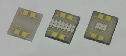
A ceramic substrate (either alumina or aluminum
nitride) is used as a mechanical system carrier, to
provide electrical contact and allow for proper ther-
mal management and cooling of the LED-chips.
Substrate dimensions are 12×10 mm², with a thick-
ness of 1 mm for aluminum nitride and 0.38 mm for
alumina. The electrical wiring and solder pads are
manufactured directly onto the surface of the sub-
strates. The wiring structures are manufactured of
W/Ni/Pd/Au layers. Solder land pads with di-
mensions of 1100×1100 µm² with a spacing of
300 µm are structured on the substrate surfaces
(Figure 1). The pads are made of sputtered eutectic
gold-tin for soldering with gold-tin solder alloy or
thin film gold for the use of adhesives and soldering
with a tin-lead solder alloy [10].
Figure 1: Aluminum nitride substrates with
electrical wiring and structured eutectic gold-tin
solder layers in two design variants (7×2 LED-
chips and 3×2 LED-chips).
IMAPS/ACerS 8th International CICMT Conference and Exhibition (2012) | April 16-19, 2012 | Erfurt, Germany
000239
Downloaded from http://meridian.allenpress.com/imaps-conferences/article-pdf/2012/CICMT/000238/2360912/cicmt-2012-tp61.pdf by guest on 03 January 2023
UVA emitting indium-gallium-aluminum-nitride
LED-chips SL-V-U40AC by Semiled Inc. with a
center wavelength of 395 nm, a chip size of
1070×1070 µm² and a rated typical optical output
power of 210 mW to 250 mW are used. The initial
design was based on NS375C-3SAA LED-chips by
Nitride Semiconductor Co., Ltd. with a chip size of
600×600 µm² but was changed to the former due to
considerations of wavelength, optical output power
and availability. The Semiled chips are available
with a back metal gold layer usable for soldering
and adhesive bonding.
Electrical contacting of the front contact is con-
ducted by ultrasonic assisted wedge-wedge wire
bonding of Au and AlSi wires. Back-side contacts
are connected by the solder or the conductive adhe-
sive to the wiring structures on the substrate. Sub-
modules are mounted to a scalable and liquid-
cooled heat-sink by means of indium foil. The use
of indium allows for a proper thermal contact and
excellent cooling due to its high ductility and its
high thermal conductivity of 82 W/(m·K).
Thermo-mechanical and thermal simulations
Based on the design data and the NS375C-3SAA
LED-chips thermal and thermo-mechanical
analyses are conducted by finite elements si-
mulations (FE). Thermo-mechanical analysis is
used to evaluate the stresses to substrate, LED-
chips and joining material due to different
coefficients of thermal expansion. Thermal analysis
provides insight in the capability of the design and
material selection on efficient heat removal from
the chips. FE analysis is computed using ANSYS
11.0 SP1.
Targeted design goals are 80 mW optical output
power and 100 mW respectively. The LED-chips
achieve 80 mW optical at 200 mA, 4.5 V and about
9.5% efficiency resulting in a thermal load of
840 mW. 100 mW optical are attained at 350 mA,
5 V with less than 6% efficiency and a resulting
thermal load of 1650 mW. A ¼-model with sym-
metric boundary conditions is used for simulation.
Base temperature of the substrate is set to 0°C and a
natural convection with 10 W/(m²·K) is applied to
all outer surfaces. Table 1 shows relevant material
properties used for the simulations. Additionally
temperature dependency for Young’s modulus,
Poisson’s ratio and plasticity of the gold-tin solder
are modeled.
Modeling soldering using eutectic AuSn with a
solder layer of 10 µm is done. Solidification of the
solder alloy from solidus to room temperature leads
to a shrinking of about 5%. Resulting mechanical
stresses within the solder layer are near the yield
strength of the material indicating plastic defor-
mation of the solder. Maximum values of 320 MPa
for AlN and 337 MPa for Al
2
O
3
are calculated.
Stresses within the base materials are computed to
be 93 MPa for AlN and 95 MPa for Al
2
O
3
which is
significantly below the ultimate tensile stresses for
those materials.
Table 1: Material properties for simulation
model (sources: [21], [22], [23] and respective
data sheets,
(1)
┴
C-axis).
Property λ TCE E ρ
Unit W/K·m ppm/K GPa g/m³
Al
2
O
3
24 6.8 340 4.0
AlN 180 4.7 320 3.3
Sapphire 40 5.4
(1)
430 4.0
Au80Sn20 58 16 59 14.7
Adhesive 17 30 1.21 3.2
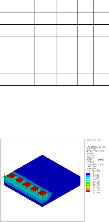
Thermal analysis is conducted to provide results of
temperature distribution and heat flux within the
sub-assemblies. For the design goal of 100 mW
optical output power per chip and a thermal load of
1.65 W chip temperatures are calculated to be 23 K
above substrate temperature for AlN and 40 K for
Al
2
O
3
using 10 µm AuSn solder layers (Figure 2
and Figure 3).
Figure 2: Temperature distribution within LED-
chips and AlN substrate (thickness 1 mm) for
eutectic AuSn solder (layer thickness 10 µm) and
1.65 W thermal load.
Calculations are repeated with respect to a con-
ductive silver-loaded thermoplastic/thermoset adhe-
sive with a thermal conductivity of 17 W/(m·K).
Assumed thicknesses of the adhesive layers are
10 µm and 30 µm respectively. Substrate material
is Al
2
O
3
with a thickness of 0.38 mm. Thermo-
mechanical strain is mainly influenced by the base
material and not the adhesive. Equivalent stresses
are 43 MPa for both adhesive layer thicknesses.
IMAPS/ACerS 8th International CICMT Conference and Exhibition (2012) | April 16-19, 2012 | Erfurt, Germany
000240
Downloaded from http://meridian.allenpress.com/imaps-conferences/article-pdf/2012/CICMT/000238/2360912/cicmt-2012-tp61.pdf by guest on 03 January 2023